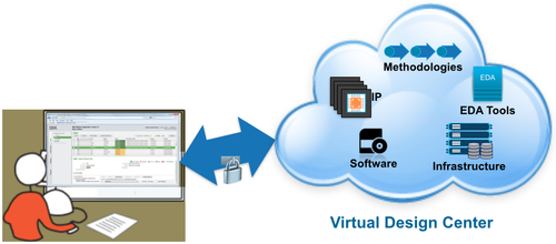
PORTLAND, Ore. — By moving its electronic
design automation (EDA) suite of chip-designing tools to the cloud, IBM
can now share its famous proprietary EDA tools with chip designers at
what it claims is one-half the price of licensing tools from other EDA
providers. Using its own SoftLayer cloud infrastructure to securely
store its tools, IBM is now offering its EDA toolkit through the SiCAD
Inc. (Cupertino, Calif.) portal — a silicon design platform provider of
cloud-based EDA design flows.
"We are targeting small- to medium-sized businesses, with a
factor of two in price/performance compared to other tool vendors,"
Christopher Porter, IBM high-performance computing (HPC) manager told EE
Times. "We now offer a pay-as-you-go business model instead of a
three-to-five year license agreement like the other EDA vendors."IBM's tools are rented per day, per application, per core — a price that will halve the cost of developing a new integrated circuit (IC), according to IBM. However, IBM is not offering the complete design flow — even internally they have to use third-party tools to complete a design — but they are offering what they say is 70-to-90 percent of a typical EDA design flow including its Library Characterization Tool (for synthesis, sign-off timers and power analysis that it claims doubles performance over competitors), its Logic Verification tool (that verifies and debugs VHDL and Verilog designs 10-times faster than competitors tools, it claims), along with its own Spice simulator.
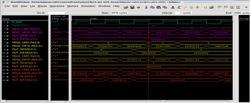
IBM is offering its proprietary verification, library characterization and Spice tools for rent (pay-as-you-go).
(Source: IBM)
(Source: IBM)
According to IBM the tools it is offering through SiCAD offer verification, simulation and regression testing, which is about 70 percent of the typical new IC design flow today and will become 90 percent of the typical design flow in the future as the industry progresses to more advanced nodes.
"The number of design rules is going up and thus the complexity of designs is going up, making our tools more and more important to the semiconductor design flow," Porter told us.
IBM also claims that it has invest over 50-to-100 years of research and development into its tools and have been using them internally for 10-to-20 years on real-world chip designs by more than 1,000 engineers on as many as 500,000 jobs producing over 100 unique mainframe and Power microprocessors, interconnects, application specific integrated circuits (ASICs) and more. Other EDA toolkits are relative newbies in comparison, IBM claims.
IBM claims its verification tool runs 10-times faster than other industry verification suites.
(Source: IBM)
(Source: IBM)
Each user will be assigned its own server for both physical and network isolation including firewalls and other proprietary techniques for securing clients data. Clients need only workstations to access the complete design flow toolkits of SiCAD, with no requirement for licenses, data centers or IT staffs.
http://www.eetimes.com/document.asp?doc_id=1326801
No comments:
Post a Comment