L attice Semiconductor Corp (LSCC.O),
a U.S. maker of programmable chips in mobile phones and tablets, is
exploring a sale that has attracted interest from a prospective Chinese
buyer, according to people familiar with the matter.
The
sale process could be a further test of corporate China's ability to
snap up U.S. chip makers, after attempted deals by Unisplendour Corp Ltd
(000938.SZ)
and China Resources Microelectronics Ltd were dropped this month on
concerns the United States could block them on national security
grounds.
Lattice
Semiconductor's sale discussions are also another example of the wave of
dealmaking sweeping the industry, fueled by a drive by major consumers
of chips, such as Apple Inc (AAPL.O) and Samsung Electronics Co (005930.KS), to cut costs.
Lattice Semiconductor is working with investment bank Morgan Stanley (MS.N)
to review interest from potential buyers, including a Chinese party,
the people said on Friday. There is no certainty Lattice Semiconductor
will agree to any deal, the people added.
The Chinese party's
identity could not be immediately established. The sources asked not to
be identified because the sale process is confidential. Lattice
Semiconductor and Morgan Stanley offered no immediate comment.
Based
in Portland, Oregon, Lattice Semiconductor makes programmable logic
chips and related software used in everything from smartphones to cars.
It has a market capitalization of about $678 million.
Earlier this week, Unisplendour scrapped its planned $3.78 billion investment in U.S. hard-disk maker Western Digital Corp (WDC.O) after the U.S. Committee on Foreign Investment (CFIUS) decided to review the transaction.
A Chinese
consortium that included China Resources Microelectronics also lost a
$2.5 billion bid to acquire Fairchild Semiconductor (FCS.O) earlier this month. Fairchild cited the risk of CFIUS blocking that deal for its decision.
Lattice
Semiconductor has been working to integrate Silicon Image, a U.S.
company it bought for $600 million in its biggest-ever deal last year,
which expanded its products for video customers.
Lattice
Semiconductor Chief Executive Darin Billerbeck said on an earnings
conference call earlier this month that he expects the first quarter "to
represent a low point" of the year for the company.
Lattice
Semiconductor blamed its weak quarterly revenue on Samsung, one of its
biggest customers, and its peers struggling with profitability and
cheaper phone models.
Twenty years ago the electronics industry became interested in the
notion of formalizing re-use through third-party IP. It has turned out
to be harder than anyone imagined.
In 1996, the Virtual Socket Interface Alliance (VSIA)
was formed to standardize the development, distribution and licensing
of IP. Soon afterward, companies with a couple of people in a garage put
up their IP developer shingle to enter the gold rush. Quality suffered,
and the industry quickly developed a bad reputation. Additional effort
was soon placed on defining the set of expected deliverables that should
go along with an IP block. That set of deliverables continues to be a
moving target. Even today, the industry is poised for the next set of
requirements that potentially will define a new set of directions and
capabilities for the industry.
Few of the original IP developers remain. Most were consolidated into
a handful of large suppliers. One that is still in business is Digital
Core Design (DCD), based in Poland.
“We have been part of the IP market since 1999, so we remember the times when the IP
market was created,” says Tomeq Cwienk, PR manager for DCD. “For us,
the design process was never about developing an IP block, selling it
and forgetting about it. Every single core we build was tailored to the
project needs.”
Since that initial effort, the IP industry has undergone a
fundamental change. “Twenty years ago when an IP block was purchased,
such as a USB block, the integrator understood the protocol themselves
and they just wanted IP for it,” notes Kevin Yee, product marketing
director for Cadence. “Today when they buy IP they don’t know much about the protocol.”
This is a key change for IP, which increasingly looks like a black
box. But for this scheme to work, the vendor has to selectively expose
aspects of the IP so it can be properly used and integrated. “SoC
design these days is less about design and more about integration,”
continues Yee. “Twenty years ago a PCI block was a good percentage of
that die, but today it is a very small part of the design. The number of
IP blocks used in a design is increasing exponentially. It used to be 1
or 2 blocks. Now it is possibly 50 or 60 blocks.”
With this change comes an associated migration of knowledge and a
change in the development schedules. IP frequently is developed in
parallel with the SoC rather than ahead of time. “There are two key
challenges that we constantly face,” says Prasad Subramaniam, vice
president of research and development and design technology for eSilicon.
“There is schedule pressure because the IP is a prerequisite for the
chip to happen, and you have to make sure that they are of good quality.
You’re often building IP that is compliant to certain standards and
oftentimes these standards are evolving, or they are not so
straightforward to interpret because you’re reading a 500-page document
and you want to make sure you pick up all the nuances that are described
in the standard.”
Another major change is related to the size and complexity of the IP
blocks. “Just as the scope of the chips has changed, IP has moved up the
food chain as well,” says Yee. “Where we used to have a simple IP
protocol, it is now much more complex, more software around it.
Integrators need to understand different things about it.”
That means that the IP has to be developed differently. “You have to
build in a lot of flexibility into your IP,” adds Yee. “Otherwise you
are building a custom IP every time and that model doesn’t work. A lot
of companies that used to develop their own IPs have switched to
third-party IP. A lot of customers use multiple nodes and multiple
processes and that means that maintenance becomes more difficult.”
The deliverables expected for an IP block can vary a lot depending
upon several aspects of that block. The first distinction is whether the
block is a hard or soft core, and the second is if it whether it is
considered to be library IP, standard interface IP or star IP. (A more
detailed description for each of these can be found in the Knowledge
Centers (Intellectual Property, Hard IP, Soft IP, Digital IP).
IP developers have been integrating greater amounts of functionality
into a single block. Examples include complete audio or video
subsystems. That could help relieve SoC integrators from having to worry
about certain aspects of the design. “Today, there is a big requirement
for security and we see this from all angles – automotive, Internet of Things etc.,” says Andrew Faulkner, senior director of product marketing for Sidense. “Because of this we are adding more features that allow our One Time Programmable
(OTP) memory to hook seamlessly into security systems and to co-operate
with various different security strategies. In addition, we are adding
capabilities such as saving secure keys and locking those keys while
minimizing or preventing side-channel attacks. It has gone from
providing a memory to adding system-level features.” New deliverables
In order to make some of the IP blocks more black box, alternative ways
must be found to provide the information that is needed for SoC
integration, such as information about quality and the ways in which the
block can be used. “One big advancement has been in coverage,” says
Gabriel Chidolue, verification technologist for Mentor Graphics.
“Integrators would like to see how the IP provider has verified what
they are delivering and that it meets the specification. Another
requirement is for ease of configuration and concepts such as IP-XACT
have come a long way in helping IP consumers leverage IP in many
different contexts. It defines how you connect IP blocks together and
how to hook it up to a verification environment.”
There are multiple viewpoints as to what needs to be exposed.
“Another view that comes out of that is a machine understandable view of
all of the registers that are inside of the block,” adds Drew Wingard, chief technology officer at Sonics.
“There is technology that takes that and creates the databook version
of the chip. Just the register description of some chips can be more
than 3,000 pages long, so automating that can be a big deal.”
The newest enabler for exposing information about the power
capabilities of a block and its external needs comes with the latest
release of IEEE 1801-2015, often called UPF.
“With UPF 3.0 it becomes possible to add a power model deliverable,”
continues Wingard. “Now with any tool that understands UPF 3.0, you get
an unambiguous description of it that could be used to calculate how
much power could be consumed in different modes of operation.”
Navraj Nandra, senior director of marketing for IP in Synopsys
adds more detailed aspects of it. “UPF is used to model retention,
isolation, power switching and power gating. UPF is the plan of record
for all our IP.”
It all comes down to providing the right information to enable the
SoC integrator to do their job more efficiently. “When you take a
concept such as power, they realize they understand the flow from a
functional point of view if everything is powered from the same supply,”
explains Chidolue. “However, if I start breaking things up into
multiple power domains, the system integrator need a little bit more
guidance about the internal functional behavior.”
There are many issues that need to be resolved. “The point here is
that the vendors must take responsibility for ensuring their IP works in
external environments, and this is hard to do,” asserts Dave Kelf, vice
president of marketing for OneSpin Solutions.
“It is not enough to deliver an integration documentation that
describes the necessary integration steps. The vendor must provide a
complete environment that can be configured to operate in the foreign
territory of their customer’s design.” Characterization
Several industries place additional demands on IP providers. “Recently,
IP consumers have become more concerned about IP reliability and ease of
integration into the ASIC,” says Vamshi Krishna, senior IP field
application engineer at Open-Silicon.
“Because to this, there is a demand for additional deliverables such as
silicon characterization reports, certifications, evaluation boards
along with the standard deliverables.”
Characterization places additional pressures on the food chain. “Our
silicon has to be qualified in advance of the SoC doing their
integration,” says Sidense’s Faulkner. “That is not always possible
because it takes a similar amount of time to qualify the IP as it does
an IC. There are 1,000 or 2,000 hours of reliability testing. It has to
go to the fab. It has to be packaged and then tested. This can be quite
lengthy. We are finding that we have to work very closely with the
foundries. We have to create PDKs and SPICE
models, and that means a high degree of risk because if we are
developing our solution at the same time as them, then this is a
conundrum that we have to find a way through.”
Depending upon the type of IP, characterization can become an even
bigger problem. “Generally, for hard IP we would like to have models at
various operating conditions, slow process, fast process, typical
process; low temperature, high temperature,” says Subramaniam. “For
certain types of IP, such as digital, the corners can be limited to
worst case condition, but for analog IP we would like to have many
corners.” Growing software content
When you look at charts of development effort, it is not uncommon to see
software being defined as requiring more time and effort than hardware
for complex SoCs these days. But the increase in software content for IP
has been more limited. “Software refers to device drivers and possible
some application layers,” says Krishna. “The investment for this
software IP block is low and, in general, do not exceed the investment
on hardware.”
There are also not quite the same quality constraints for this
software. “You need to deliver drivers with your IP, so that there is a
reference,” says Larry Lapides, vice president of sales for Imperas.
“But how can you keep up with having Linux, FreeRTOS, VxWorks, ThreadX
and so on. You can’t do them all, but you do need to have one or two
reference implementations.”
Part of the reason for the slow software growth is the nature of the
IP targets. “The software component right now is probably small, and
it’s unclear to me whether it will grow,” says Subramaniam. “This is
because if you’re trying to target a hardware IP block you probably want
to put more and more into the hardware to get the most out of it, and
therefore the software component of it should be small.”
Wingard agrees for most cases. “We don’t see the software content
exceeding hardware any time soon for most IP blocks. But in media, it
might be true today. Audio subsystems have to deal with a large number
of compression and decompression standards and things like echo
cancelation. These tend to be written in software. People who have done
well in this area probably have spent more on software than hardware. In
graphics, it is probably about there. In video, decoders and encoders
are sufficiently challenging hardware designs, so it is probably on the
edge there. The other place may be security. Hardware security could
include RSA, DES and all of the other crypto function. So they may be
close to having more software than hardware.”
But while the IP may not need large quantities of software, there is a
growing need to run software on a model of the complete SoC, and that
may mean additional models being requested. “While software may be a
significant component of the IP,” says Lapides, “what is more important
is having the high-level models for integration verification and you also need the fast untimed models for software development.”
Additional models can be added to that list. “Some IP can impact the
performance of the design and thus the desire to deliver a performance
model of the IP,” says Wingard. “This may help the customer to make sure
that the collection of blocks has enough performance, when combined
together, with all of the other things that are all working together, to
share resources to such things as memory. Sometimes that performance
model is fairly simple and at other times it might looks like the
description of traffic associated with this block along with the time
domain view of it.”
One thing is blazingly clear. The IP market is a work in progress and
the demands placed on the industry are increasing all of the time. It
is no longer possible to develop a hardware block and expect it to be
adopted by the industry. The role of IP is to help and decrease the
workload on the SoC integrator and that requires a very large amount of
collateral be provided along with the functionality.
MediaTek wasted no time at the Mobile World Congress and
showcased two new SoC models, namely the Helio P20 for smartphones and
the MT2511 for bio-sensing wearables.
The Helio P20 follows in the steps of P10, a mid-range CPU
targeted at tablets and smartphones. It sports ARM's state of the art
Mali-T880 GPU. Helio P20 is an octo-core CPU, with Cortex-A53 cores
running at 2.3GHz.
MediaTek used the 16 nm FinFET Plus (16FF+) process to manufacture
the chipset, switching from the previous 28 nm standard. This enables
the CPU to go as high as 2.3 GHz instead of only 2 GHz.
According to the OEM, the new chip consumes 25 percent less power than its predecessor, Helio P10. Not only that, but MediaTek says that the GPU offers 25 percent more performance in video and gaming apps.
Helio P20 is a premiere, being the first SoC that works on Samsung's
LPDDR4X RAM module. This offers increased bandwidth over the LPDDR3, by
as much as 70 percent.
Another notable upgrade in the P20 is that it offers WorldMode LTE
Category 6 support alongside 2x20 carrier aggregation, enabling it to
download files at 300 Mbps and upload them at 50 Mbps.
Dual-SIM fans will be happy to know that the SoC has global standby
for two SIMs, as well as multicast service backed by LTE multimedia. The
LTE multimedia support lets users get HD video content over LTE
connections.
"Helio P20 meets today's consumer demand for sleek, powerful yet highly power efficient mobile devices," says Jeffrey Ju, executive vice president and co-chief operating officer at MediaTek.
Ju points out that multimedia activities and battery life are among
the most important criteria for consumers, and his company manages to
offer both to a high standard.
Helio P20 SoC equipped gadgets will start shipping in Q2 of 2016.
MediaTek provides SoCs for midrange smartphones, the most notable example being HTC One M9s.
MediaTek also revealed the MT2511, the first foray of the company
into "bio-sensing analogue front-end (AFE) chip." The MT2511 should give
processing power to fitness and health devices. MediaTek touts that
power efficiency of the chip is unmatched.
The MT2511 eliminates the interference and motion artifacts when it
collects the electrical signals of the heart. It accomplishes this by
using high sample rate from 64 to 4 KHz and a 100db dynamic range.
The chipset is able to store pulse data, making it an asset in pulse
oximetry (SpO2), electroencephalography (EEG), electromyography (EMG)
and blood pressure analysis.
Both the 'Internet of Things' and wearable industry will want to use
the MT2511 in devices such as active lifestyle smart watches, fitness
trackers or sports bands. MediaTek announced that the manufacturing
stage for the MT2511 starts during the first half of the year.
"We can only begin to imagine how health-related wearables will
improve both medical care and everyday wellness all around the world," says JC Hsu, MediaTek's Corporate VP and GM of the IoT business unit.
Hsu goes on to add that the mobile health market leads the technology field in terms of growth quickness.
Are you excited about the new chipsets from MediaTek? Let us know in the comment section below.
The U.S. hard-disk maker, Western Digital Corp (WDC.O), said on Tuesday that China's Unisplendour Corp Ltd (000938.SZ)
had scrapped its planned $3.78 billion investment in the company, a
move that in turn alters the terms of Western's deal for rival SanDisk
Corp (SNDK.O).
Unisplendour,
a unit of China's state-backed Tsinghua Holdings Co Ltd [TSHUAA.UL],
dropped its plan to buy a 15 percent stake in Western Digital after the
U.S. Committee on Foreign Investment (CFIUS) said it would investigate
the transaction.
As a
result Western Digital will now present an alternative offer for SanDisk
consisting of more Western Digital stock and less cash, the companies
said, giving the deal an overall value of $15.78 billion. The original
agreement, struck in October, valued the deal at $19 billion.
The
collapse of the Unisplendour deal comes during a wave of Chinese
takeover interest in U.S. corporations that has already hit a record of
$23 billion in announced offers this year, according to Thomson Reuters
data. That is nearly double the full-year record reached in 2013.
But
China's ambitions in the U.S. are receiving increased scrutiny from
U.S. politicians, who are concerned about putting certain national
businesses in the hands of Chinese executives and government officials.
Western
Digital said last October that it would revise the cash-and-stock offer
for SanDisk if the Unisplendour investment in Western Digital was not
successful.
"It was understood
that there was a possibility that the Unis investment in WDC may not
happen," said Sumit Sadana, SanDisk Executive Vice President. Sadana
said that the value of the deal for Sandisk is now $78.50 per share,
down from $86.50 when it was originally struck.
Both companies have said they are committed to the agreement, which is expected to close in the first half of this year.
Western
Digital's stock price has fallen from around $80 per share last October
and fell another 7.2 percent to $42.77 on Tuesday.
"I
think if you are a Western Digital shareholder, the deal makes a lot of
strategic sense," said Pacific Crest Securities analyst Monika Garg.
ACTIVIST SHAREHOLDER
Western
Digital's move to proceed with the SanDisk deal comes the day after
shareholder Alken Asset Management urged the company to scrap it, saying
the price was too high.
"We have
laid out our case in reasonable details in the letter so there is not
much to add," Alken analyst Vincent Rech said in an email. The
London-based fund is pleased with the support it has received, he added.
Western Digital said U.S., European Union and other regulators had approved the SanDisk deal.
CFIUS, an
inter-agency panel led by the U.S. Treasury Department, assesses
potential mergers to ensure they do not endanger national security. The
panel rarely kills the deals, but several times a year it has informally
urged companies to scrap merger plans and they have complied.
China
led the countries whose planned U.S. acquisitions and investments for
2014 were probed for security issues, according to a government report.
In January, Philips (PHG.AS)
dropped a plan to sell an 80 percent stake in its Lumileds division to a
group that included Chinese investors because of pressure from CFIUS.
Fairchild Semiconductor International Inc (FCS.O)
said last week that it rejected an offer from a Chinese takeover group,
citing concerns that U.S. regulators would stop the sale.
U.S. lawmakers are also pushing for the rejection of a Chinese company's plan to buy the Chicago Stock Exchange.
he outlook for China’s semiconductor manufacturers and
mobile parts makers is beginning to look up, thanks to rising consumer
demand and government backing for more internet connectivity in
lifestyles, even as a tough competitive environment remains, analysts
say.
Mobile phone handset shipments in China rose 5 per cent year-on-year
in January to 49.4 million units, according to statistics published by
the Ministry of Industry and Information Technology.
Of those, smartphone shipments were up 10.3 per cent to 44.59
million. In December, the monthly net increase in LTE subscribers
exceeded 30 million for the first time, reaching 386 million in total.
“It appears that the switchover from 2G/3G to 4G (LTE) has begun to
accelerate in earnest,” wrote Nomura analysts in a note last week,
forecasting smartphone shipments of 40 to 45 million units per month in
2016 versus 38 million in 2015.
The benefits of market growth haven’t flowed directly through to
smartphone component manufacturers. Jefferies analyst Ken Hui points out
that smartphone makers Huawei and Xiaomi have added pressure to an
already competitive market with increased insourcing and in-house
development.
“We expect in-house development to mostly impact [Taiwan-based]
Mediatek, which shipped around 20 million chips to Xiaomi in 2015,” Hui
said, citing Xiaomi plans to develop a chip based on technology licensed
from Chinese semiconductor maker Leadcore Technology.
The outlook is better for other manufacturers, with Hong Kong-listed
Semiconductor Manufacturing International Corporation (SMIC) attracting
“buy” and “outperform” ratings from Jefferies and Daiwa respectively.
SMIC beat fourth quarter projections by growing revenue 7 per cent
quarter-on-quarter to US$610 million (HK$4.74 billion), although its
gross margin was below consensus due to research and development costs
and price competition.China
is expected to announce this year plans to build an internet of things
infrastructure overlaying the existing mobile network. Illustration by
Craig Stephens
“2016 looks to be a transitional year for SMIC, which is shifting
focus from profit to sales growth,” said Daiwa analyst Rick Hsu. “We
expect SMIC’s earnings to rebound sharply in 2017, after the
transition.”
Jefferies described SMIC as an “invest for the future” company based
on its aggressive capacity expansion plans and acquisitive stance, along
with successful product lines like its fingerprint sensor.
But with China’s smartphone market maturing, analysts covering the
communications chips sector are turning their attention to the bigger
opportunities promised by the “internet of things”, the network of
physical objects, including devices, vehicles and buildings, that
contain electronics, software, sensors and connectivity, enabling them
to collect and exchange data.
The trend was described by former premier Wen Jiabaoas an “emerging
strategic industry”. The Ministry of Industry and Information Technology
forecasts the market value of China’s internet of things to reach 1
trillion yuan (HK$1.19 trillion) by 2020, up from 200 billion yuan in
2010.
“Logistics companies, utilities and manufacturers, in particular, are
increasingly harnessing the real-time information provided by
connectivity to increase efficiency, lower costs and better manage
infrastructure,” said a report from mobile operators industry group
GSMA.
The technology also has applications in the healthcare and food
safety sectors, and Beijing plans eventually to extend it into remote
locations nationwide, supported by bandwidth aggregation and device
platform sharing among the big three mobile operators.
“We expect some China government bodies to announce a massive plan
later this year to build an internet of things infrastructure overlaying
the existing mobile network in the next few years.” Hui said.
“The internet of things network will gradually give birth to terminal
devices, thus creating demand for a lot of chips. Although these chips,
transmitting at about 200Kbps, have lower values, the market is
incremental with huge volume potential.”
According to Jefferies, Shenzhen semiconductor maker HiSilicon, ZTE
Corporation’s microelectronics arm and US firm Qualcomm have already
begun development. It also said Hong Kong-listed ASM Pacific Technology
and SMIC are poised to benefit.
After teasing the chip module for nearly a year, Samsung has finally
commercially launched its ARTIK Internet of Things (IoT) platform, with a
partner program to promote it and Digi-Key as its online distributor.
amsung has finally commercially launched its ARTIK family of chips for IoT businesses after unveiling them last May in San Francisco.
ARTIK
is a one-stop chip module that has a built-in application processor,
modem chip, memory chip, and sensor, as well as supporting software,
drivers, storage, security, development board, and cloud in the software
front. ARTIK is offered in three options with different sizes and specifications: ARTIK 1, ARTIK 5, and ARTIK 10.
Its
diverse support for numerous technologies allows developers and product
designers freedom to build "whatever device they want", a Samsung
spokesman said.
Developer kits for the chip can be ordered from Samsung's channel
partner Digi-Key Electronics starting February 22 and those wishing to
utilise the chips for their devices can go to the official homepage and order in bulk. Lower volume orders can be placed on Digi-Key's website from sometime next month.
Samsung
also launched the Certified ARTIK Partner Program. Those who place
orders and join will get support from the tech giant to accelerate
commercialisation of their products that use the chip. In terms of
operating systems, ARTIK offers support for Snappy Ubuntu, Tizen,
Canonical, Fedora Linux stack, and Nucleus Real Time, but not Android.
In
tools, Arduino's web-based development environment and Temboo, which
enables cloud connectivity and automatic code generation, will be
supported. Medium One's workflow tools and voice control of Sensory and
Soundhound, as well as 3D radar tech by Vayyar are available.
Clients
get to use Microsoft's Azure cloud platform as well as Samsung's own
SAMIIO, an open data exchange platform. Samsung stressed that the chips
have built-in hardware security with trusted executive environment (TEE)
by Trustonic.
"I'm very proud of the Samsung ARTIK team and the
strong momentum they have achieved. In less than 8 months, we've gone
from product launch to commercial availability, while building multiple
modules, operating systems, embedded security, and a growing ecosystem
of actively engaged partners," said CTO Dr Byungse So of Samsung
Strategy and Innovation Center, in a statement.
"We believe in the power of open platforms and partner ecosystems,
leveraging the wealth of expertise and experience available in the
market to bring delightful experiences to our customers. We're excited
to see all the innovative projects that developers will come up with in
the future."
The South Korean tech giant has repeatedly promoted
IoT since last year's Consumer Electronics Show. The topic is likely to
be a big part of the upcoming Mobile World Congress in Barcelona, as well as for tech companies in general.
Samsung declined to comment on expected volume and revenue from the business.
http://www.zdnet.com/article/samsung-commercialises-artik-chip-in-iot-push/
The sensor is more powerful and energy efficient, and provides a more
accurate heart rate reading compared with similar modules, the company
has said.
G Innotek, the components-making affiliate of LG Group, has come out
with an ultra-thin sensor module for monitoring heart rate, blood
oxygen, and stress levels.
The heart rate monitoring module packs a
photodiode, LEDs, and its integrated circuit into a slim 1mm module,
and according to the company utilises embedding technology from the PCB
industry to reduce the size of the sensor module.
The module is
also 30 percent more powerful, making accurate detection of biometric
signals easier, and 20 percent more energy efficient compared with
similar modules, the company said.
For example, its new heart rate monitoring sensor improves the
accuracy of health tracking wearables to ±5bpm (beats per minute) during
exercise from ±8 in current devices. So, if the user's heart rate is
120bpm, the heart rate measured by the wearable device would give a
reading of between 115bpm to 125bpm, as opposed to one from 112bpm to
128bpm.
"At the heart of the Internet of Things are the sensors
that enable the sharing of information. We are developing these
high-tech sensors for use in automobiles, consumer electronics, and
wearable devices to lead the IoT industry," said Kim Chang-hwan, senior
vice president and head of the Components and Materials R&D Centre.
LG
Innotek is the world's largest manufacturer of camera modules,
specialising in components for the mobile, automotive, and semiconductor
industries.
The key to wearable technology is reducing the size
of a device and increasing power efficiency. No matter how good a
feature is, if a wearable device is bulky and the battery wears out
rapidly, it will never become popular. We're likely to see developments
like this one as the wearables market heats up even more.
HONG
KONG — As Chinese companies try to snap up American tech businesses,
they are setting off ripples of unease in the Obama administration and
in Congress, inciting a backlash that has stopped the latest acquisition
attempt.
One
of the companies that first brought silicon to Silicon Valley —
Fairchild Semiconductor International — said it would remain in American
hands after rejecting a takeover offer worth about $2.5 billion led by
Chinese state-backed buyers. Instead, Fairchild embraced a smaller bid
from an American rival on Tuesday, citing concerns that federal
regulators might reject the Chinese deal.
The
unsuccessful Chinese bid for Fairchild was just one of at least 10 such
offers in the last year for international semiconductor businesses,
mostly in the United States. China’s Five-Year Plan, the government’s
economic and strategic road map, has emphasized semiconductors as a core
industry. And a long list of Chinese companies with varying ties to the
government have been trying to acquire foreign technology in the
sector.
Recent
Chinese moves in areas like heavy equipment, aerospace and financial
services are also drawing attention from both ends of the American
political spectrum.
A
group of 44 Republican members of Congress and one Democrat sent a
letter on Tuesday afternoon to the Treasury Department, demanding that
the Obama administration’s interagency committee on foreign acquisitions
“conduct a full and rigorous investigation” of a bid by a company in
Chongqing, China, to acquire the small but historic Chicago Stock
Exchange.
Representative
Robert Pittenger, Republican of North Carolina, said in a telephone
interview that it had been easy to gather signatures on the letter in
the House, with members worried that the deal would give China direct
access to America’s financial infrastructure. “It took two days —
generally, you’ll spend two weeks trying to get signatures,” he said.
But because semiconductors are the tiny electronic cores of a long list of military systems, including drones
and smart bombs, Chinese interest in them has attracted the most
attention in Washington. Those worries have been amplified as the Obama
administration has repeatedly accused Beijing of cyberespionage against
the United States. The worries have further increased as China has
expanded its role in the South China Sea, including claims by the United
States and Taiwan this week that China has deployed surface-to-air missiles there.
“China’s
engaged in a buying spree of international semiconductor firms,” said
Michael R. Wessel, a member of the United States-China Economic and
Security Review Commission, a group created by Congress to monitor
bilateral relations. “What they can’t develop on their own, they intend
to buy, if they can, or steal, if they must.”
The
Chinese government has vehemently denied that it is responsible for
hacking attacks, while pointing to detailed disclosures by Edward
Snowden of how the United States engages in extensive electronic
intelligence gathering on China. Economists in China — and some in the
United States, particularly at Wall Street banks that advise on Chinese
acquisitions — argue that the United States needs to remain open to
foreign investment, particularly given low American savings rates.
When
Washington politicians start objecting to Chinese acquisitions,
“they’re caught up by old-school, Cold War thinking,” said Fred Hu, a
prominent Chinese economist and fund manager.
Fears
about Chinese control over critical technologies recently prompted
United States officials to block a $2.9 billion deal for Chinese
investors to buy a controlling stake in a unit of the Dutch electronics company Philips.
Fairchild
said in early January that it expected a bid from China Resources
Microelectronics — a unit of the state-owned China Resources Holdings —
and Hua Capital Management to be a “superior proposal.” That offer
amounted to $21.70 a share in cash, compared with the $20 a share that ON Semiconductor,
an American company, had on the table. But worries about the likelihood
of approval from the Committee on Foreign Investment in the United
States outweighed the attractiveness of the bid.
Fairchild’s
decision shows the effect of broader political suspicion in the United
States toward Chinese investment in the high-tech sector. Last summer, a
similar but much larger deal was derailed before it even made it to
regulators. The $23 billion bid
for the American memory chip maker Micron by a Chinese state-controlled
firm was undone by concerns about its political feasibility.
In
that case, Senator Chuck Schumer, Democrat of New York, voiced worries
about the deal’s effect on national security in a public letter to
Treasury Secretary Jacob J. Lew. But Republicans are now starting to
take up the issue, which means that it could take on a partisan
dimension in an election year.
Despite
the difficult climate, Chinese bids for American companies seem likely
to increase, affected by a slowing Chinese economy and a desire by many
Chinese companies to move money out of the country before China’s
currency can weaken further against the dollar. In the sensitive
microchip industry, deals are also being driven by more than $100
billion set aside by the Chinese government to help the country improve
the sophistication and scale of the critical industry.
The
number of deals involving a Chinese company that is trying to buy an
overseas chip maker rose to 21 last year, including the offer for
Fairchild, from eight in 2010, according to the data company Dealogic.
There have already been five this year, worth $857 million.
That
has drawn more attention to the Committee on Foreign Investment in the
United States, also known as Cfius. An interagency body that includes
representatives from the Treasury, Justice and Defense Departments,
Cfius can recommend against foreign deals made for American companies,
or companies connected to the United States, on grounds of national
security. The agency can also broker compromises in which companies
enact special security checks for sensitive aspects of an acquisition or
sell off those assets.
Many in the semiconductor industry are watching closely to see whether Cfius will investigate a bid by the Chinese chip maker Tsinghua Holdings for a stake
in the American company Western Digital, which makes hard disk drives. A
lack of an investigation could herald more moves by Chinese investors
to take minority stakes in American chip and memory companies.
The potential Chinese buyers of Fairchild had already agreed to pay a $108 million termination fee
if the deal did not get approval from Cfius. They also increased their
offer to $22 a share after Fairchild raised concerns. But Fairchild’s
transaction committee said an agreement would still be too risky.
The
Fairchild board said in a regulatory filing on Tuesday that it found
the higher offer attractive but that there was “nonnegligible risk of a
failure to obtain Cfius approval.”
Fairchild
works on several technologies that could have raised concerns. In
particular, it develops and produces sensors that track motion in three
dimensions, which are used in many cutting-edge technologies. Xsens,
a company acquired by Fairchild in 2014, works on sensors that guide
unmanned submarines and drones and help in maritime surveillance.
Shares
of ON Semiconductor closed up more than 6 percent on Tuesday, when
Fairchild announced that it still favored the American company’s bid.
Fairchild’s stock dropped almost 3 percent.
Taiwan Semiconductor Manufacturing Company (TSMC) on
February 6 estimated wafer shipments in the first quarter of 2016 would
decrease less than 1% due to the impact of a large earthquake hitting
southern Taiwan in the early morning of February 6, but on February 12
indicated that the decrease in wafer shipments will be more than 1%,
because damage to Fab 14 is worse than originally assessed.
TSMC
originally estimated that more than 95% of foundry machines could be
restored to normal conditions in 2-3 days following the earthquake.
Machines at Fab 6 and Fab 14B have already been fully restored, the
company said.
Despite the earthquake, TSMC said it is
confident of hitting target consolidated revenues of NT$198-201 billion
(US$5.9-6.0 billion) for the first quarter of 2016.
Panel
maker Innolux indicated that the earthquake did not damage 3.5G and 4G
factories, but did affect 5G and 6G factories at STSP, with restoration
estimated to take a week. Innolux has shifted partial production from
factories at STSP to a factory in northern Taiwan to minimize the impact
on shipments, the company said.
In a bid to minimize
the impact of earthquakes, the STSP administration will cooperate with
the National Center for Research on Earthquake Engineering under the
government-sponsored National Applied Research Laboratories to set up an
earthquake early warning system and disaster information and analysis
mechanism.
TORONTO—2016 may be shaping up to be the year
memory makers commit to upping 3D NAND production in a bid to replace
its planar predecessor.
Micron announced its 3D NAND technology is now available in
multi-level cell (MLC) and triple level cell (TLC) products, and expects
by the second half of the year that the majority of its total NAND
flash output to be on 3D NAND as designers build devices such as
laptops, tablets and servers that need its increased capacity,
performance and power.
SSDs are the obvious opportunity for 3D NAND, said Kevin Kilbuck,
Micron's director of NAND strategic planning, particularly enterprise
storage. The company is sampling 3D NAND-based client SSDs this month
that will be generally available in June. It will also find its way into
embedded markets such as automotive, industrial, and mobile devices as
well as Internet of Things devices, he told EE Times in a telephone
interview.
Micron has begun volume production of 256Gb MLC and 384Gb TLC that
can be stacked and put into an SSD. Kilbuck said Micron can get 3.5 TB
into an m.2 form factor and 10 TB in a 2.5-inch form factor. He said
Micron has made some architectural innovations to further reduce the
cost of 3D NAND, noting that XY lithography is now becoming irrelevant.
“3D NAND sets the clock back. We are able to relax the XY lithography.
It's how high can you stack it."
One of the changes Micron was able to make was the ability to hide
more than 75% of the CMOS logic under the array with its 32-tier 256Gb
MLC/384Gb TLC 3D NAND products.
Kilbuck said Micron chose to stick with floating gate technology,
which has been around since the early days of flash and used for EEPROM
and NOR, noting there have been issues with the charge trap approach,
such as charge loss which affect retention. “We didn't want to have to
solve those issues while stacking." It made sense to stack a known
entity, he said, rather than exponentially stretch the learning curve.
“It was a matter of de-risking our schedule and deployment plans."
Micron has begun volume production of 256Gb MLC and 384Gb TLC 3D NAND for SSDs that can get 3.5TB into an m.2 form factor.
What will also contribute to 3D NAND's uptake in 2016 is that there
is a supporting ecosystem for the technology, said Kilbuck, with
companies such as PMC Sierra and Silicon Motion providing controllers.
Silicon Motion introduced a turnkey merchant SATA SSD controller supporting 3D NAND
from multiple vendors, including Micron, earlier this year at CES. It
supports provisioning of higher capacity SSDs, from a broad range of
vendors, up to 2TB.
Kilbuck said Micron staff responsible for ecosystem enablement
started visiting controller partners a couple of years ago to share and discuss its roadmap for 3D NAND.
While 3D NAND is often labelled as revolutionary because of its
potential for reduced cost and increased density, Kilbuck said in many
ways, including from a controller standpoint, it's just a natural
evolution from its predecessor. "It's still NAND to the controller.
There may be a few more features to deploy but it's still fundamentally a
pretty evolutionary change for them."
There are several controllers ready to handle Micron's 3D NAND
depending on the market segment for flash cards, client SSD and
enterprise SSDs, said Kilbuck. The initial densities Micron is
manufacturing are well above what is used in embedded applications.
Meanwhile there is lots of room for SSD growth in the notebook segment,
he said, and the enterprise space as organizations still haven't
completely moved away from spinning disk in the data center.
Kilbuck said 2016 is the year of 3D NAND, but more specifically, it's
an investment year as vendors look to ramp up and make it more
cost-effective to produce than 2D NAND. “Planar is hitting the end of
its wall. There are still a few more shrinks left."
He acknowledged there are tradeoffs when moving to 3D NAND—there are
more process steps and wafer costs go up. “Once you get some scale
behind it, no wants to be on the old technology." Micron announced with Intel
last March that together they would be second to Samsung with
ultra-dense 3D NAND flash chips that will sell as chips and in SSDs. Not
long after, Toshiba announced it was shipping samples of its 48-layer 3D Bit Cost Scalable (BiCS) stacked cell structure flash.
Qualcomm has had quite the busy day today. After unveiling its new Snapdragon Wear 2100 chipset built with Android Wear
devices in mind, the company has now taken the wraps off four new
products that are likely to make a splash in the mobile industry.
First, Qualcomm announced
three new additions to the mid- and low-end Snapdragon lineup, the
Snapdragon 625, 435 and 425. Unsurprisingly, the Snapdragon 625 is the
highest-end out of the bunch. As the successor to the 617,
the 625 features two quad-core clusters of Cortex A53’s and is clocked
at 2GHz, up from its predecessor’s 1.5GHz clock speed. It also comes
with an Adreno 506 graphics processor.
The Snapdragon 435 is next up on the list. This one replaces the Snapdragon 430,
which was only unveiled a few months ago alongside the 617. The new 435
is an octa-core Cortex-A53 CPU and is the first in its class to
integrate the X8 LTE modem, which supports 4G+, and 2x20MHz carrier
aggregation for faster downlink and uplink LTE speeds. It’s clocked at
1.4GHz and comes with the Adreno 505 GPU. The Snapdragon 425 is a
quad-core Cortex A53 CPU clocked at 1.4GHz and featuring an Adreno
308 GPU. This lower-end processor is aimed at replacing the Snapdragon
410 and 412.
For more detailed information on these three new SoCs, take a look at the press release in the source link below.
Qualcomm has also announced the mobile industry’s first Gigabit Class
LTE modem, the Snapdragon X16 LTE. The X16 LTE modem is built on a 14nm
FinFET process, and is designed to produce fiber-like LTE Category 16
download speeds of up to 1 Gbps, supporting up to 4x20MHz downlink
across FDD and TDD spectrum with 256-QAM, and 2x20MHz uplink and 64-QAM
for speeds up to 150Mbps. It’s important to note that the X16 LTE is
ahead of its time, and the mobile network providers we have today don’t
even come close to offering speeds of 1 Gbps. Qualcomm says
with Gigabit Class LTE speeds, users will be able to take advantage of
features such as live streaming 360-degree VR content and faster access
to cloud-based apps and services.
Heat is becoming a much bigger problem for semiconductor and
system design, fueled by higher density and the increasing use of
complex in markets such as automotive, where reliability is measured in
decade-long increments.
In the past, heat typically was handled by mechanical engineers, who
figured out where to put heat sinks, fans, or holes to funnel heat out
of a chassis. But as more functionality is added onto a PCB or into an
SoC, heat is becoming a much more important consideration at the silicon
level—one that is difficult to predict, manage, and risky to ignore.
“Thermal has always been a problem, but it’s gotten worse as the
chip, board and enclosures have gotten smaller,” said Greg Caswell,
senior member of the technical staff at DfR Solutions, a reliability
engineering services firm. He noted this problem has become noticeably
worse in the past year. “We’re finding solder fatigue, plated hole
fatigue, parts being mixed with different coefficients for expansion. If
it needs underfill, that underfill doesn’t necessarily match up with
the other parts. There are about 700 laminates to keep track of, and it
all can change depending upon the type of board material. People say
they’re using FR-4 boards, but there are 400 materials catalogued as
FR-4. Over a period of 10 years, you start finding diurnal stresses,
shock and vibration problems, weird temperature variations, and lots of
different voltage levels. All of this plays into the ability of a
product to survive.”
Survival is a relative term. Many designs now have to be fully
functional for much longer periods than in the past because of demands
for extended reliability in end markets such as automotive, aerospace,
medical, industrial. Even chips in an automobile’s infotainment system
needs to last 10 to 15 years because of possible interaction with
safety-critical systems.
“In a mobile device, the typical active life is 5,000 hours,” said Ron Moore, vice president of marketing for ARM‘s
Physical IP Division. “For a server, it’s 100,000 hours. You need to do
extra EM analysis, more analysis on flip-flops. So the physical IP is
changing according to the physical requirements.”
This isn’t exactly a new topic of discussion for semiconductor engineers. In 2001, Pat Gelsinger—then Intel‘s
CTO—predicted that within a decade the energy density of chips would be
equivalent to the surface of the sun if nothing was done. The solutions
came in the form of multiple cores, dark silicon methodologies, new
materials, and a number of of very good engineering and design
techniques. But the problem has never went away, and it has come back
with a vengeance in finFET-based
designs, particularly at the next couple of process nodes, forcing
companies to consider 2.5D and fan-out packaging, new architectures and
microarchitectures, and raising questions about the long-term impacts of
even modestly higher temperatures.
“Thermal adds a whole bunch of unknowns,” said Aveek Sarkar, vice president of product engineering and support at Ansys.
“You need to assess the thermal impact at the chip-package and system
levels, at the chip level or the interconnect level, and if it’s a
finFET you have to deal with localized heating. At 10nm and 7nm this is
going to get worse. You have to predict what will happen with power, and
then create temperature profiles for different power scenarios.”
Temperature is relatively steady state, compared with spikes in
voltage drops, for instance. That makes it deceptive to deal with
effectively. It should seem logical that, in conjunction with the
thermal conductive properties of silicon, the heat should dissipate
across and out of a chip. But in a densely packed SoC, not all of that
heat can escape. Wherever that channel gets blocked, it can overheat
components, sometimes completely on the other side of the chip.
“What’s changed is that now you need to consider thermal management
closer to silicon,” said Robin Bornoff, FloTherm and FloVent marketing
manager at Mentor Graphics.
“If you look at the infotainment systems in automobiles, the
environment is quite extreme. There is heat in the dashboard, and it’s
hard for that heat to leave. There are not many cooling channels. That
can cause the IGBT
to experience radical changes and make it unreliable under certain
driving profiles. It also can have an effect on digital displays, where
the brightness changes or the color changes. We’re talking about large
temperature gradients. For bond wires, which handle a large amount of
power, there is a thermomechanical risk of bond wire failures.” Predicting problems
Figuring out when and where thermal issues will crop up requires a combination of tools, history, and a healthy dose of luck.
“Everything might look okay, but 35 seconds into a simulation you
find a power problem that’s generating thermal issues,” said Alan
Gibbons, power architect at Synopsys.
“You need a very accurate model with more details of what’s going on.
But you don’t want to have to run it for the whole 35 seconds. So you
swap in a more accurate functional model that is cycle-accurate, find
the power hotspot, and then back out and move on.”
Things don’t always work out that well, though. “You may find a
thermal issue in the core due to a software task on the wrong process or
something is being done in software when it should be done in
hardware,” Gibbons said. “This is a big challenge for the EDA community.
We normally think about reliability in terms of power and performance,
but it can be affected by power densities. If you have processors
running at 2 to 3 GHz they dissipate a lot of power. Thermal
considerations become more acute.”
This becomes even more problematic at advanced nodes, because
margining costs power and/or performance. With less of a buffer, designs
need to be more exact. But one of the goals of SoCs is fitting more
functionality into a given space, so there are more variables in terms
of use models.
“Modeling and simulation scenarios are different,” said Ansys’
Sarkar. “You have to understand under which conditions a function is
operating. And you have to put that in context of the whole chip. So the
chip may show 80° C, but it is no longer uniform so you have to
recalculate the power for the temperature profile. An ARM block might be
85° and an instruction cache might be 75°. Calculating temperature is
an iterative process between temperature and power. Once you get the
temperature profile, then you have to figure out whether it’s too
pessimistic or optimistic based up the lifetime of the chip. If you look
at foundry electromigration rules, they say you get a 10-year life if
you follow the rules, which have a certain temperature. If the
temperature increases from 110° to 125°, the chip will fail faster.”
But with uneven temperatures across a die, it’s much harder to calculate the impact on reliability.
All of the major EDA companies are now working on this problem.
“Traditionally, analysis tools have focused on package temperature,”
said CT Kao, product engineering architect at Cadence.
“But with a 10nm finFET, you don’t have the granularity you need to go
from the PCB to the transistor. What’s needed is a physics analysis
simulation. At the chip level, we can resolve place and route inside a
chip and combine that with thermal. So we have granularity in that
direction, but not directly for the PCB.”
What’s difficult to nail down is exactly what different engineers
need at different times, even for the same design. Some need a detailed
thermal analysis of transistors or groups of transistors, while others
only need a system-level analysis. “And all of this has to be combined
with experiments and good engineering judgment,” said Kao. “You don’t
necessarily need to know the temperature of individual transistors if
they’re next to each other, but you do need to know how chips behave
under different functional requirements and how hot they are over time.” Solutions
FinFETs have provided a respite from leakage current at 16/14nm, which
has been increasingly difficult to manage since 65nm. But the problem
begins to grow again, starting at 10nm, and that drives up heat.
“Leakage didn’t go away and semiconductor physics is not changing,” said Drew Wingard, CTO at Sonics.
“For one node it has become less important. What we’re seeing now is a
lot more emphasis on clock control for power management. But the reality
is that a large chunk of power is still in the clock tree. Another
challenge is dynamic power management. There is no automation, so you
need to work at the micro-architectural if not the architectural level.”
All of this has a direct impact on heat. The more things that are in
the ‘on’ state, and the longer they remain on, the more heat they
generate and the greater the thermal effects. Wingard said one solution
is better clock control, because clocks can be turned off and start up
in one clock cycle, which is very quick. “You can arrange power
management in groups, so you turn them on in sequence. You also can turn
on smaller ones first, so the inrush current is spread over a longer
period of time. Then when you turn on the fat transistors, there is
lower resistance.”
Advanced packaging is another option, and one that has gained more
attention over the past year as high-bandwidth memory solutions began
hitting the market. But there are plenty more options there, including
how the individual die are packaged together.
“One of the key issues is thermal dissipation,” said Craig Mitchell,
president of of the Invensas business unit of Tessera. “That changes
depending on the thickness of the die. If you reduce the thickness you
can reduce the resistance to pull more heat out.”
Tessera has begun developing a different way of stacking DRAM, as
well, staggering the die the way bricks are staggered, so that on every
stack a portion of the DRAM is open. That approach allows more cooling
and with shorter interconnects and faster memory access.
Also on the memory front, companies such as Kilopass have been
working on one-time programmable memory as an alternative to other types
of non-volatilve memory because of its resistance to heat. “Unlike
embedded Flash memory, OTP handles extreme heat well,” said Jen-Tai Hsu,
Kilopass ‘
vice president of engineering. “Both do okay with cold temperatures as
low as -40° Celsius. But OTP works to 125° Celsius, while embedded Flash
memory typically only supports to about 85° Celsius. With mechanical
areas in the car reaching extreme temperatures and a need for memory
that doesn’t fail, OTP is a better choice.”
There also has been a significant push to eliminate the problem in
the first place. Mentor’s Bornoff said there has been research into new
areas such as thermal through-silicon vias,
as well, which act like chimneys out of a package. “The challenge is
that if you experience any bottleneck, it backs up all the way to the
heat source. The best way to deal with that is to transfer heat close to
the source. The use of thermal vias is well established, but dedicated
thermal TSVs is an area of active research. We still need to understand
how many are needed and how those factor into design. But it could have a
massive impact on the rest of a design.”
Bornoff said liquid channels etched on the underside of a die are
another area of active research. So are new thermal interface materials.
“We’re seeing new ones coming into play that use small parts of metal
suspended in a substrate. Material science is helping here. We can do
thermal simulation based on the thickness of materials and their
different properties. Temperature is always a good leading indicator of
failure mechanisms.” Other issues
Heat has other effects that are just beginning to be understood in the
semiconductor world as it crosses into the world of deep physics.
“One strong impact of higher temperature, when combined with high
voltage, is an increased risk of latch up, and this is a serious
reliability issue,” said Olivier Lauzeral, president and general manager
of iROC Technologies, another reliability engineering services company.
“Another impact from temperature is the actual flux of thermal neutrons
in the room. These neutrons interact with Boron 10 dopants in silicon
to produce alpha particles and lithium ions. The cross section (or
probability of interaction) of thermal neutrons with Boron 10 varies as
1/√E, with E being the energy of the neutron which is positively
correlated with temperature (hence the term thermal neutrons). So the
higher the temperature, the higher their energy, the lower the
probability of interaction with ^10B, the lower the flux of alpha or
lithium ions.”
Heat has been responsible over the past year for more bit slips and
data retention problems in flash memory, as well, according to Edward
Wyrwas, senior member of the technical staff at DfR Solutions. “We’re
also seeing the effects on gate oxide integrity and we’re seeing more negative bias temperature instability
(NBTI). And as components like graphics cards begin doing more critical
thinking, and we start using more memories and more FPGAs, temperatures
will go even higher.”
Those problems will likely be compounded as the Internet of
Everything begins kicking into gear, because many devices will need to
be always on, and as more features are added into systems that can be
affected by different use models. Both can affect heat.
“What’s necessary here is that you design chips so they accomplish a
certain workload,” said ARM’s Moore. “So you’re making predictions as
you’re analyzing reliability in a set of workflows. Maybe this
application will drive nearly overload voltage. This is more of an
implementation issue, but it’s an increasing trend. Implementation is
more and more important, and it affects where you are in your margin.”
The bottom line is that thermal issues are increasingly part of the
design, and need to independently and in conjunction with power,
materials, architectures, processes and packaging. On a positive note,
this does provide some very interesting multi-physics engineering
problems to solve for years to come.
While it’s definitely nice that the new HDA125 digital analyzer from Teledyne LeCroy
zips along at 12.5 GSamples/s on 18 input channels, a closer look shows
that the story is more about addressing real-world embedded test and
validation problems in the most practical and cost-effective manner
possible.
Of course, that’s what all test vendors strive to accomplish. Nothing
strange there, so you’d be forgiven for moving along at this point, but
hang on a second. Yes, the sampling rate is high, and note too that the
HDA125 is an external box that connects to any Teledyne LeCroy scope
via the proprietary LBUS interface to synch triggers and timebases to
the picosecond (Fig. 1).
1.
The HDA125 is a high-speed mixed-signal analyzer and probe system that
operates as an add-on to the Teledyne LeCroy WaveMaster line of scopes
so you can get the functionality without buying a whole new mixed-signal
oscilloscope.
That approach is also what grabbed my attention: modular is smart as
it leverages the installed base of oscilloscopes to cater to current
users’ needs, and helps keep costs down and provides flexibility. The
system would typically be matched to one of the company’s WaveMaster 4-
to 30-GHz scopes.
Then I noticed that the HDA125 itself costs up to $20,000 if you
ordered a full, 18-channel leadset. That’s when I realized there was
much more to the HDA125 than appeared at first blush.
Obviously, going from a regular DSO to an MSO has a cost differential
associated with it. According to Teledyne LeCroy’s Patrick Connally,
technical marketing engineer for high-bandwidth oscilloscopes, the cost
differential is in the same ballpark as the cost of the full HDA125,
“except you don’t get the lead set: and that’s a pretty high-tech piece
of equipment.” He added that with competitors’ standalone MSOs, “that
can be an extra $7,500 to get the bandwidth needed for [the high-speed]
sample rate to be useful.”
Read more at: http://electronicdesign.com/blog/hda125-mixed-signal-probe-tackles-real-world-test-issues
NAND flash memory has surpassed hard disk drive (HDD)
technology in areal density for the first time, according to a new
report from a market research firm.
During a presentation at the 2016 IEEE International Solid State Circuits Conference
(ISSCC) in San Francisco last week, Micron shared data showing NAND
flash has moved past HDDs in areal density, according to Coughlin
Associates.
At last year's ISSCC, Samsung white papers
indicated that its 3D NAND flash products had reached 1.19Tbits per
square inch (Tbpsi) and said in 2016 they would reach 1.69Tbpsi.
This
year, Micron revealed it had demonstrated areal densities in its
laboratories of up to 2.77Tbpsi for its 3D NAND. That compares with the
densest HDDs of about 1.3Tbpsi. Tom Coughlin, Coughlin Associates
president, noted the flash advancements in a column in Forbes.com last week.
The
announced hard drive products from the third quarter of 2014 to the
third quarter of 2015 had an increased areal density of about 60%, So
HDDs have not stopped evolving," Coughlin said.
"On the other
hand, flash memory is getting denser with technology announcements of
2.77Tbspi, higher than any announced HDD areal density. This is a new
development. So flash is developing and certainly getting competitive in
terms of areal storage density, but the chips are still more expensive
to make than disks and the raw costs of storage will likely remain less
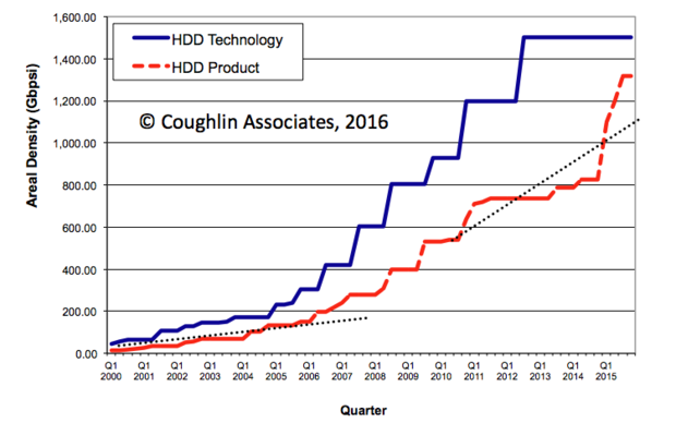
for HDDs for some time to come." ASTC, Samsung
During its presentation this week at ISSCC, Samsung representatives
referenced an Advanced Storage Technology Consortium graphic that
projected HDD areal density out to the years 2025. Samsung superimposed
its own timeline on the graphic, and said that in 2015 NAND flash had
already surpassed magnetic head storage technology (HDD and magnetic
tape drives) in areal density.
If you're still relying on conference calls or one-to-one instant messaging, it's time your team Read Now
The
highest areal density for today's HDD products is about 1.3Tbpsi,
according to Coughlin. Most HDD products, however, are well below that.
For example, Seagate's desktop hard drives have a maximum areal density
of 850Gbpsi; those drives use shingled magnetic recording (SMR), which
overlaps the magnetic tracks for greater density.
While still
best-case laboratory figures, the NAND flash areal densities shown at
the ISSCC are not far behind what is shipping today. Major SSD makers,
such as Samsung, have announced what would be industry-leading 15TB 2.5-in solid-state drives (SSDs) are already on the horizon.
Tokyo-based Fixstars is selling
a 13TB, 2.5-in SSD that will be selling for $1 per gigabyte -- or
$13,000. By comparison, an 8TB helium filled hard drive can be purchased
for as little as $515.
During
its presentation this week at ISSCC, Samsung representatives referenced
an Advanced Storage Technology Consortium graphic that projected HDD
areal density out to the year 2025. Samsung superimposed its own
timeline on the graphic, and said that in 2015 NAND flash had already
surpassed magnetic head storage technology (HDD and magnetic tape
drives) in areal density. Coughlin Associates
HDD products continue to increase in areal density. The highest HDD
technology demonstrations date from 2012 at about 1.5 terabits per
square inch (Tbpsi). HDD areal densities today in shipping products,
however, are only as high as 1.3Tbpsi. "That doesn't mean that the price is going to
reach parity with hard drives because the factories to build flash are
still a lot more expensive to build than the hard drive factories --
especially the 3D NAND; it's something like a $10 billion plant,"
Coughlin said.
Because of 3D NAND's greater density,
manufacturers such as Micron and Intel are opening new plants or are
revamping older NAND facilities to increase their 3D production, which
is driving prices down.
According to a recent report
by DRAMeXchange, a division of market research firm TrendForce, the
plummeting prices of SSDs have also driven their recent adoption in
laptops. This year, SSDs will be used in around one-quarter of laptops.
Next
year, SSDs are expected to be in 31% of new consumer laptops, and by
2017 they'll be in 41%, according to DRAMeXchange senior manager Alan
Chen.
While SSD pricing has dropped dramatically
over the past three years, HDD pricing hasn't. From 2012 to 2015,
per-gigabyte pricing for HDDs dropped just one cent per year -- from 9
cents in 2012 to 6 cents this year. However, through 2017, the
per-gigabyte price of HDDs is expected to remain flat at 6 cents per
gigabyte.
In 2013, Samsung became the first semiconductor
manufacturer to begin producing 3D NAND. Its V-NAND chip provided two to
10 times higher reliability and twice the write performance of planar
(single-layer) NAND products, the company claimed at the time.
Samsung's
V-NAND uses a cell structure based on 3D Charge Trap Flash (CTF)
technology that allows V-NAND to provide more than twice the scaling of
today's 20nm-class planar NAND flash.
Last year, SanDisk and Toshiba announced
they had begun manufacturing 256Gbit (32GB), 3-bit-per-cell, 48-layer,
3D NAND flash chips that offer twice the capacity of the next densest
memory.
Coughlin believes 3D NAND products will reach price parity
with the more common planar NAND by 2017. But he's skeptical that any
type of NAND flash will reach parity with HDDs anytime in the near
future.
"It's possible, but that requires hard-drive makers to
quit trying to increase their capacity," Coughlin said. "They're still
putting R&D dollars into shingled and two dimentional magnetic
recording. So I don't think all the magnetic storage industry's tricks
are out of the bag yet."
For example, Seagate's CTO Mark Re said in an interview with Computerworld
in November 2014 that his company plans to begin using heat-assisted
magnetic recording (HAMR). This technology uses a laser to help
stabilize bits written to a platter, and will increase density by as
much as 40%.
Using HAMR, the theoretical density for hard drives
skyrockets, affording a 3.5-in server or desktop drive up to 60TB and a
single-platter, 2.5-in. laptop drive up to 20TB of capacity.
Seagate has already demonstrated HDDs using HAMR with areal densities of 1.4Tbpsi, Re said.
The
company plans by next year to be "working with a select partner or two
to demonstrate a product in a data center application, and in 2018
you'll see HAMR technology used more broadly in the field," Re said.
 China
is expected to announce this year plans to build an internet of things
infrastructure overlaying the existing mobile network. Illustration by
Craig Stephens
China
is expected to announce this year plans to build an internet of things
infrastructure overlaying the existing mobile network. Illustration by
Craig Stephens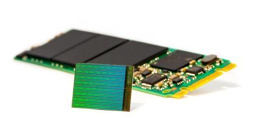

 That approach is also what grabbed my attention: modular is smart as
it leverages the installed base of oscilloscopes to cater to current
users’ needs, and helps keep costs down and provides flexibility. The
system would typically be matched to one of the company’s WaveMaster 4-
to 30-GHz scopes.
That approach is also what grabbed my attention: modular is smart as
it leverages the installed base of oscilloscopes to cater to current
users’ needs, and helps keep costs down and provides flexibility. The
system would typically be matched to one of the company’s WaveMaster 4-
to 30-GHz scopes. ASTC, Samsung
 Coughlin Associates
 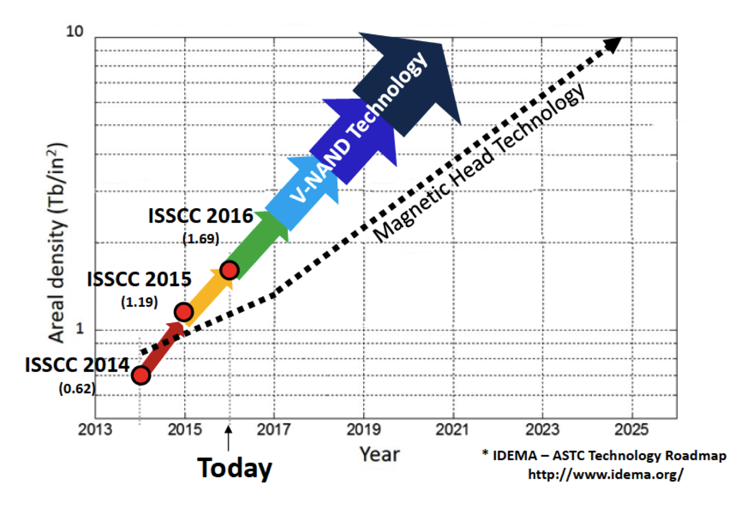 ASTC, Samsung
  Coughlin Associates