Tuesday, May 31, 2016

Globalfoundries Forms Joint Venture to Make More Chips in China


Globalfoundries Inc., one of the largest contract manufacturers of semiconductors, is forming a joint venture with the government of Chongqing to get greater access to the Chinese chip market.
Globalfoundries will re-equip an older plant in the inland Chinese city with production aimed for 2017, the company and the local government said Monday in a statement. Chongqing is furnishing land and the existing facility, while the company will provide tools to upgrade it to 300-millimeter from 200-millimeter wafer production, making it more efficient. It won’t get the most up-to-date technology the Silicon Valley-based company uses in its U.S. facility.
Chip companies are moving production to the world’s largest market for semiconductors, responding to China’s push to domesticate manufacturing and replace imports that rival oil in the amount of money they suck out of the country. By shifting plants there, overseas chipmakers are hoping to keep access to important customers such as Chinese electronics makers.
“China is the fastest-growing semiconductor market, with more than half of the world’s semiconductor consumption and a growing ecosystem of fabless companies competing on a global scale,” Globalfoundries Chief Executive Officer Sanjay Jha said in the statement. “We are pleased to partner with the Chongqing leadership to expand our investment in support of our growing Chinese customer base.”
Created from elements of Advanced Micro Devices Inc., Chartered Semiconductor Manufacturing and International Business Machines Corp., Globalfoundries is owned by the investment arm of the government of Abu Dhabi.
http://www.bloomberg.com/news/articles/2016-05-31/globalfoundries-forms-joint-venture-to-make-more-chips-in-china

Friday, May 27, 2016

Intel acquires computer vision startup Itseez for Internet of Things and self-driving cars

Intel has acquired computer vision startup Itseez for an undisclosed price as it moves further in the Internet of Things and automotive electronics markets.
Doug Davis, senior vice president of the Internet of Things group at the world’s biggest chip maker, said in a blog post today that “Intel is transforming from a PC company to a company that powers the cloud and billions of smart, connected computing devices. These devices will use the power of Intel technology to process data being generated from ‘things,’ connect to and learn from data being analyzed in the cloud, and deliver amazing new experiences.”
One of the Internet of Things (making ordinary objects smart and connected) projects that Intel is gearing up for is self-driving cars. Davis noted that Americans spend some 75 billion hours a year driving. Morgan Stanley estimates that self-driving vehicles could deliver $507 billion in annual productivity gains — to cite just one of the compelling benefits, he wrote.

“While the possibilities are exciting, the reality requires solving a myriad of technology challenges,” Davis wrote. “Solutions will need to seamlessly deliver a combination of compute, connectivity, security, machine learning, human machine interfaces and functional safety.”
Intel is adding new capabilities in cars such as functional safety and over-the-air software management, as well as the ability to see surroundings and interpret them.
Computer vision includes methods for acquiring, processing, analyzing, and understanding images from the real world in order to make informed decisions and automate actions. Computer vision technology is quickly becoming critical for the future of smart and connected “things” in autonomous vehicles, security systems, medical imaging, and more, Davis said.
Itseez creates software and integration for everything from cars to security systems. Davis said Itseez will become a key ingredient for Intel’s Internet of Things Group (IOTG) roadmap, and will help Intel’s customers create applications like autonomous driving, digital security and surveillance, and industrial inspection. Itseez is also a key contributor to computer vision standards initiatives including OpenCV and OpenVX.
“Together, we’ll step up our contribution to these standards bodies — defining a technology bridge that helps the industry move more quickly to OpenVX-based products,” Davis wrote.
In an interview with VentureBeat, Davis said that the Internet of Things has a few phases. It has to make everyday objects smart. It has to connect the unconnected. And it will enable devices to make real-time decisions based on their surroundings in an autonomous fashion.

http://venturebeat.com/2016/05/26/intel-acquires-computer-vision-startup-itseez-for-internet-of-things-and-self-driving-cars/

Thursday, May 26, 2016

GloFo Looks For 7nm Leadership

A pretty big shift could be about to happen in the semiconductor industry – IBM’s scientific prowess could be about to be unleashed on the market.
GlobalFoundries is aiming to take industry process technology leadership at the 7nm node.
For the first time, GloFo now reckons it can take industry process leadership using a proprietary, in-house developed process technology , and this is thanks to the IBM acquisition.
“The IBM acquisition gave us people experienced in leading edge development,” GLoFo’s CTO Gary Patton tells me, ” the people who developed 45nm, 32nm, 22nm and 14nm are the same people who are working on 7nm.”
As well as IBM’s process experts GloFo is also benefitting from the Albany Nanotechnology Centre who his still run by IBM but which is currently “focussing on Malta” says Patton.
“Malta (one of GLoFo’s New York fabs) is high yield on 14nm, that gives me a very solid baseline to do the next node,” said Patton.
A major step towards achieving an industry-leading process at 7nm is a 60% shrink in the 14nm to 7nm transition.
When I asked how this was achieved, Patton replied: “We’re shrinking the pitches pretty aggressively.”
Under the terms of the IBM-GloFo deal 50% of Albany’s effort is going to support Malta with the other 50% pursuing pathfinding.
GLoFo’s 7nm process is so aggressive that, says Patton, it will deliver lower wafer cost even if EUV is delayed and they have to use multiple patterning. Patton reckons that EUV will be used in production in 2020 with “small usage in the 2018/19 timeframe.”
If GloFo can pull this off, it could have a big effect on the semiconductor industry with a fourth leading-edge process technology exponent in the industry along with Intel, TSMC and Samsung.
The net effect of another source of leading edge capacity could prove to be a powerful de-consolidating force in an industry which has recently shown trends towards consolidation.

http://www.electronicsweekly.com/blogs/mannerisms/manufacturing-mannerisms/glofo-looks-for-7nm-leadership-2016-05/

Tuesday, May 24, 2016

Going the Distance with PCIe

TORONTO--One of the challenges flash-based storage has faced is that systems designers have been using hard disk architectures and applying them to SSDs, including PCI Express (PCIe).
PCIe, however, was not specifically designed for storage. Although it has a great deal of theoretical bandwidth, it has inherent limitations because it is not a native storage interface. It requires an onboard controller to manage resources between the flash memory and server I/O. And if I/O requests scale beyond controller thresholds, it can dramatically increase latency.
While that has led some vendors to develop alternative technologies, PCIe is still a widely-used interface that has advantages. And despite efforts to build more compact systems that keep everything close together to reduce the distance a signal must travel, sometimes it's not always possible.
Parade Technologies in Santa Clara, Calif., has opted to address this reality with something called a redriver. The high-speed interface IC supplier just introduced a two-lane 8Gb/s PCI Express and SATA redriver targeted at M.2 SSDs and other high speed peripheral applications. The PS8559 features four redriver channels enabling the support of two bi-directional lanes, and is able to handle PCIe up to 8Gb/sec and SATA up to 6Gb/sec.
Alan Yuen, senior director of marketing for Parade's high speed products, said sometimes the design of a system means a signal has to travel farther, which means in can degrade. Although the 8Gb/sec transfer rate of PCIe brings a welcomed performance increase, it also presents challenges to systems designers. At this speed, the allowable distance through PCB traces and other interconnect becomes limited because of signal distortion.
This is where a redriver comes in, Yuen said. “Redrivers help a transaction travel without errors," he said.
The PS8559, placed along the signal path or near the end of the path by the peripheral connector, cleans up and re-transmits the PCIe or SATA signal, both increasing data transmission reliability and enabling system design flexibility, Yuen said. For each of the four PCI Express or SATA channels, the PS8559 integrates a receiver, an adaptive filter that removes distortion and a transmitter, he added.
Parade's PS8559 is a bidirectional, two-lane signal redriver that supports PCIe Gen 3, with data rates up to 8.0 GT/s, and SATA, with rates up to 6 Gb/s.
Because it supports PCIe and SATA, the PS8559 is ideal for the SATA Express interface, which utilizes both of these interface standards and is used for PC storage devices, Yuen said. The support of two PCIe lanes also makes the PS8559 well suited for the newer M.2 interface used in PCs and laptops. Yuen noted that the PS8559 is optimized for low power and includes an automatic power saving mode, making it well suited for portable systems, while other uses include server-class PCIe SSDs as well as PCIe cabling.
Redrivers are not the only option for boosting signals, said Yuen. Retimers are also common and can handle very high speeds, but are common in larger systems. Redrivers are used more often in notebooks and tablets, he said, and to some extent, servers. They are also the most common and generally cheaper. “Redrivers have the benefit being easy to use and cost effective," Yuen said.
PCIe has the advantage of being very scalable, Yuen said. “Between number of lanes and speed per lane, you can get lot of performance headroom," he said. “From our perspective, PCIE has been very useful and widely adopted for high I/O.
The roadmap for PCIe sees products with gen 3.x available roughly from now until 2017, with gen 4 expected in 2018. Yuen said Intel is one the primary drivers of PCIe, and thus the market for redrivers as well.

http://www.eetimes.com/document.asp?doc_id=1329744

Monday, May 23, 2016

Synopsys Buys Simpleware

Synopsys bought Simpleware, which makes tools for turning 3D images into models that can be used in simulation.
The deal extends Synopsys into a spectrum of new markets, including medical, dental, oil and gas and even food sciences and archaeology. While the company still has a play in computer-aided engineering and design, Simpleware’s 3D imaging data can also be used for 3D printing.
“Simpleware has deep expertise and patented technology in 3D meshing of complex structures, which we expect will improve our capabilities to address complicated and/or large-scale TCAD simulation,” Synopsys said in a statement. “The wide range of applications enabled by the Simpleware technology provide us with the opportunity to nurture and grow new markets beyond our traditional semiconductor segment.”
Specialized simulation is seen as an increasingly attractive field for EDA companies, made possible by a massive increase in processing power, cheap memory and much faster throughput.
Terms of the deal were not disclosed


http://semiengineering.com/synopsys-buys-simpleware/

Friday, May 20, 2016

Google I/O: Google and Qualcomm demo Android embedded in a car

The functions of a concept car were demonstrated at Google I/O in California today.  They ran on a Qualcomm Snapdragon 820 automotive processor.
The plan is to have a series of Automotive Development Platforms (ADP) for Snapdragon 820A and Snapdragon 602A processors. These will be used for system development and testing.
The ADPs will be available through Intrinsyc, the Canadian embedded wireless supplier.
Patrick Brady, director of Android engineering, Google, writes:
“Google is committed to building Android into a platform that fuels innovation in the automotive space. We are in close collaboration with industry leaders such as Qualcomm Technologies, Inc. to bring the best of Android into the automobile in a safe and seamless way. This initiative represents the next step in bringing the power of an open platform and rich ecosystem that enables car makers to create powerful infotainment systems designed for the digital age.”
Nakul Duggal, vp of product management at Qualcomm Technologies, writes:
“Snapdragon Automotive processors, combined with Android, will enable the automotive ecosystem to create cutting-edge connected car and infotainment platforms. Android as the infotainment OS in the car will allow drivers and passengers to interact with their vehicles in new and exciting ways. We are pleased to be working with Google and the automotive ecosystem to usher in the next generation of in-car experiences.”

http://www.electronicsweekly.com/news/google-and-qualcomm-demo-android-embedded-in-a-car-2016-05/

Thursday, May 19, 2016

What’s Next For NAND?

NAND flash memory is a key enabler in today’s systems, but it’s a difficult business. NAND suppliers require deep pockets and strong technology to survive in the competitive landscape. And going forward, vendors face new challenges on several fronts.
On one front, for example, the overall NAND market is currently in the doldrums, amid soft product prices and a mild capacity glut. Demand is expected to rebound in the second half of 2016, although there is still uncertainty in the market.
Then, on the technology front, today’s planar NAND is reaching its physical scaling limit. And so NAND suppliers are pinning their future hopes on the successor to planar NAND—3D NAND.
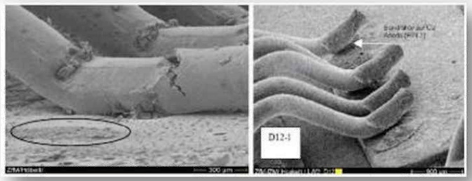
3D NAND is shipping, but the technology is taking longer than expected to enter the mainstream. It is more difficult to make than previously thought. 3D NAND resembles a vertical skyscraper, in which horizontal levels or layers are stacked and then connected using tiny vertical channels.
“The early movers, such as Samsung and Micron, are ramping up 3D NAND quickly, while SK Hynix and SanDisk/Toshiba are lagging,” said Greg Wong, an analyst with Forward Insights. “The technology and yield learning is taking longer.”
And it isn’t getting any easier. Today’s leading-edge 3D NAND chips are 32- and 48-layer devices, but the technology will likely hit the ceiling at 128 layers in the 2018 timeframe or so. So to extend 3D NAND beyond 128 layers, vendors are quietly developing a technology called string stacking. Still in R&D, string stacking involves a process of stacking individual 3D NAND devices on top of each other.
For example, a vendor might stack three separate 48-layer 3D NAND devices, creating a 144-layer chip. Even with string stacking, though, 3D NAND could hit the wall at 300 layers. It will take vast resources and capital to extend current and futuristic 3D NAND devices to 128 layers and beyond. “Scaling the number of layers is not just a technical challenge, but an economic one as well,” Wong said.
In any case, OEMs will need to keep close tabs on the technology. To help OEMs, Semiconductor Engineering has taken a look at the status of the following technologies—planar NAND; 3D NAND; and futuristic 3D NAND with string stacking.
Planar NAND
Invented in the 1980s, NAND flash is a nonvolatile memory technology that can be electrically erased and reprogrammed. Basically, NAND is used for data storage applications. Its close cousin, NOR flash, is geared for code storage. In today’s systems, NAND plays a key role in the traditional memory hierarchy. Basically, SRAM is integrated into the processor for cache. DRAM is used for main memory. And disk drives and NAND-based solid-state drives (SSDs) and memory cards are used for storage.
The NAND market is dominated by large suppliers. (See chart below.)
Screen Shot 2016-05-18 at 10.55.20 AM
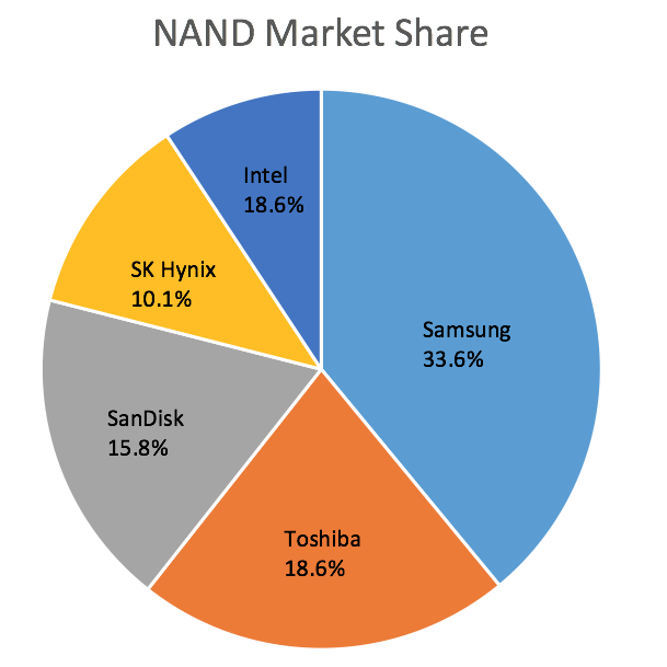
Source: Semiconductor Engineering chart compiled from TrendForce data.
In 2015, worldwide NAND revenues increased by 10%, while bit growth grew by 52%, according to Web-Feet Research. “In 2016, revenue will be flat at a 0.4% growth rate even though bit growth will come in around 46%,” said Alan Niebel, president of Web-Feet Research. “This is due to oversupply of planar NAND and price declines for mobile, consumer and some SSDs.”
Today, prices for planar NAND are inexpensive and continue to fall. Not long ago, for example, hard disk drives (HDDs) were significantly cheaper than rival NAND-based SSDs. By year’s end, the price difference between a 128-GB SSD and a 500-GB HDD will fall to less than $3, according to TrendForce.
For OEMs, though, there is a potential problem. NAND flash vendors have converted some of their planar NAND fab capacity over to 3D NAND. If demand picks up, and vendors can’t ramp up 3D NAND fast enough, OEMs could face product shortages in the second half of 2016 and perhaps beyond.
“Our outlook is for a shortage in NAND in general,” said Jim Handy, an analyst with Objective Analysis. “It all depends on whether or not people are able to overcome the technical barriers to get out 3D NAND. And it’s really hard to predict when that will happen.”
The other problem? Planar NAND is running out of steam.

Planar NAND is running out of steam, but it’s far from dead.

Planar NAND is based on a floating gate transistor structure. A NAND device, which resembles a MOSFET, consists of a source and a drain with a channel running between them. Unlike a MOSFET, there are two gates on the top of a NAND structure. A control gate is on top, while the floating gate is on the bottom. The two gates are insulated by an oxide layer.
The data is stored in a NAND cell. In single-level cell (SLC) NAND flash, there is 1 bit of data per cell. Today’s mainstream NAND makes use of multi-level cell (MLC) and triple-level cell (TLC) technology, which stores 2 bits and 3 bits of data per cell, respectively.
NAND vendors have scaled the cell size by roughly 100 times over the past decade, according to Micron Technology. In fact, thanks to advanced lithography, vendors have extended planar NAND down to the mid-1xnm node regime.
Today, NAND vendors are shipping 16nm and 15nm parts. But at those nodes, NAND is running of out of gas and it will no longer scale. It is becoming difficult to scale the memory cell and floating gate in planar NAND.
But planar NAND is not dead. “Planar NAND is not going away,” said Kevin Kilbuck, director of NAND strategic planning at Micron. “Customers want 2D NAND for the foreseeable future for let’s call it the non-high capacity storage market. Not all of the applications are moving to 3D NAND right away. And not all of the manufacturers will convert all of their capacity from 2D to 3D NAND overnight. It’s not economical to manufacture low-density products in 3D NAND fabs. It’s also very expensive to build new 3D NAND fabs or covert 2D NAND fabs to 3D.”
3D NAND
Still, the future rests with 3D NAND. This technology first appeared in 2007, when Toshiba introduced the world’s first 3D NAND technology. Later, Samsung, SK Hynix and the Micron/Intel duo introduced 3D NAND.
3D NAND represents a radical departure from planar or 2D NAND. Planar NAND involves the production of horizontal strips of polysilicon. The strips are used to make the wordlines. These, in turn, connect the control gates of the memory cells.
In 3D NAND, the polysilicon strips are stretched, folded over and stood up vertically. Basically, 3D NAND involves a stack of layers. The layers are connected with tiny vertical channels. The layers, which are horizontal, are the active wordlines. “The bitlines also run horizontally in the metal layers on the top of the chip,” Objective Analysis’ Handy said. “The vertical channels are the NAND ‘strings’ that attach to the bitlines.”
There are other differences as well. Micron and its technology partner, Intel, extended the floating gate architecture to 3D NAND. In contrast, Samsung, SK Hynix and the SanDisk/Toshiba duo are not using a floating gate for 3D NAND. Instead, these vendors went to a technology called charge trap flash.
All told, 3D NAND has some advantages over planar NAND. “Compared to planar NAND, 3D NAND offers a significant bit density increase,” said Yang Pan, chief technology officer for the Global Products Group at Lam Research. “As such, there is increasing adoption of 3D NAND by SSDs as a storage solution for servers/datacenters as well as high-end consumer applications.”
Still, 3D NAND has some challenges. “From the device side, it’s the channel mobility,” said Er-Xuan Ping, managing director of memory and materials within the Silicon Systems Group at Applied Materials. “Polysilicon does not have good mobility.”
In 3D NAND, the goal is to move the current through a polysilicon-based vertical channel. A 3D NAND device with fewer layers, and a shorter channel length, might have acceptable mobility.
Problems can arise as vendors scale their devices with more layers, meaning the channel length becomes taller. “When you go up, the polysilicon channel will be limited by its mobility,” Ping said.

Mobility is affected by the number of layers.

In addition, 3D NAND involves a number of new and complex process steps in the fab. Planar NAND is dependent on advanced lithography. In contrast, 3D NAND makes use of trailing-edge geometries from 40nm to 20nm. 3D NAND requires lithography, but the challenges shift from advanced patterning to deposition and etch.
Despite the challenge, 3D NAND is set to take off. In 2015, the overall 3D NAND market reached $4.5 billion in terms of sales, according to Web-Feet Research. “In 2016, 3D NAND will come in big time with both Toshiba and Micron producing volume shipments, thereby growing worldwide bit shipments by 350% and revenues by 230%,” Web-Feet Research’s Niebel said.
Each vendor, meanwhile, is ramping up 3D NAND at various stages. In 2013, Samsung shipped the world’s first 3D NAND device, a 24-layer, 128-gigabit (Gb) chip. Then, last year, Samsung shipped its third-generation 3D NAND device. The device is 48 layers, based on tri-level cell (TLC) technology, resulting in a 256-Gb chip.
Samsung’s previous chip was a 32-layer chip. The 48-layer device is roughly 2X to 2.2X faster in terms of a sequential read and a sequential write, according to Jim Elliott, corporate vice president of Samsung Semiconductor.
The 48-layer chip also enables Samsung to penetrate new markets, namely the enterprise SSD sector. “The big story is TLC in the enterprise space,” Elliott said. “That’s where that disruption is taking place.”
Samsung’s rivals, however, opted to skip the 24-layer regime. For most, a 16nm or 15nm planar NAND chip is still cheaper on a cost-per-bit basis than a 24-layer 3D NAND device.
Meanwhile, the Intel/Micron duo recently entered the 3D NAND market by rolling out a 32-layer device. Meanwhile, SK Hynix and the SanDisk/Toshiba duo are separately sampling 48-layer products.
The 32-layer device from Intel/Micron supports both multi-level cell (MLC) and TLC technology, enabling densities of 256- and 384-Gb, respectively. The 384-Gb chip, according to Micron, is the highest density 3D NAND device in the market.
To accomplish this feat, Micron integrated the logic circuitry under the layer stack. It refers to this as CMOS under array. “We can get the majority of logic under the array, thereby saving a lot of space. That allows more density in a given silicon area,” Micron’s Kilbuck said. “It also allows us to segment the array. It can increase the number of planes, for example. Our NAND pages are divided into four planes. What that does is increase your throughput and performance of an individual die.”
Despite the obvious benefits of 3D NAND, there is one big question: When will 3D NAND reach price parity with 2D NAND?
Today, 3D NAND is sold at a premium. The 32- and 48-layer devices are inching closer in terms of price parity with 2D NAND. But it may take chips with 64 layers and beyond to reach the magical price parity point.
“Our TLC-based 3D NAND is getting close to what 2D MLC can do in endurance,” Kilbuck said. “My gut feeling is sometime next year we would see price parity between 2D and 3D. I’m talking about price per gigabyte. But everybody needs to be in high volume (production) for that to occur.”
What’s next?
So what happens next? “This is the year of 48 layers going to 64,” Applied’s Ping said. “Whether 3D NAND can go to 96 or 128 is limited by the etching capability.”
In fact, it’s difficult to fabricate devices with 64 or more layers. Right now, the high-aspect ratio etch tools are not ready or struggling to fabricate devices at 64 layers and beyond. For now, the aspect ratios are too complex and difficult.
And at 64 layers and beyond, channel mobility becomes an issue, as previously stated. “It will limit the device performance or device height,” Ping said.
So going forward, NAND suppliers will simultaneously follow two parallel paths. The first path is to wait for the etch tools and other manufacturing techniques to arrive. And if they arrive on time, vendors could scale today’s 3D NAND device from 32- and 48-layers, to 64 layers, to 96 and then to 128.
The second path is to move towards string stacking technology. This involves stacking two or more individual devices on top each other. Each device is separated by an insulating layer.
String stacking is already in the works. Recently, Micron presented a paper on a new 64-layer chip. Micron, according to multiple sources, stacked two 32-layer chips on top of each other.
In theory, string stacking could involve several different combinations. For example, a vendor could stack three 32-layer chips, enabling a 96-layer device. In addition, a vendor could stack three 96-layer chips, resulting in a 288-layer product.
The trick is to connect the various chips together. Today, vendors are looking at several different interconnect schemes. “Some of them will put a source line in the middle,” Ping said. “That is just one of the many options.”
Clearly, string stacking is challenging. And even with this technology, 3D NAND could hit the wall at 300 layers or so. “That’s the limit,” he said. “That’s based on yield and stress.”
All told, 3D NAND will remain viable at least to 2020, and perhaps beyond. But suddenly, 3D NAND has some new competition, which complicates the landscape.
Today, the Intel/Micron duo are sampling 3D XPoint, a ReRAM-like device that could potentially compete with 3D NAND in enterprise SSD applications. ReRAM, a nonvolatile memory technology, is attractive because it delivers fast write times with more endurance than today’s flash.
There are other promising technologies in R&D, particularly vertical ReRAM. “The densities (in vertical ReRAM) won’t be as high as 3D NAND,” Ping said. “But the speeds can overcome some of these density limitations.”
Time will tell if ReRAM will displace 3D NAND. In fact, ReRAM and the other next-generation memory types still have a lot to prove. At one time, the newfangled memory types were supposed to replace conventional memory, but they have fallen short of their promises. And conventional memory, such as DRAM and NAND, continue to chug along.

http://semiengineering.com/whats-next-for-nand/

Wednesday, May 18, 2016

Broadcom buys Israeli 5G co MagnaCom for $60m


The Petah Tikva based company has developed 5G technology to alleviate congestion and satisfy bandwidth demand.


Semiconductor connectivity giant Broadcom has acquired Israeli startup MagnaCom, which develops 5G wireless communications technology. A spokesman for MagnaCom has confirmed the acquisition for "Globes" but did not disclose financial details about the deal. Market sources believe that Broadcom is paying $60 million for the Petah Tikva based company.
Broadcom, which was recently acquired by Singapore's Avago, has a market cap of $56 billion and has 8,200 employees worldwide including 700 in Israel, resulting from a dozen previous acquisitions in the country.
MagnaCom was founded in 2012 by CEO Yossi Cohen and CTO Amir Eliaz and has raised $8 million to date. The company has 20 employees.
The company was founded around a whole new, patented modulation technology called WAM, which can help alleviate the global spectrum congestion and insatiable demand for more bandwidth. WAM can be adapted in cellular, Wi-Fi, satellite and cable TV, wireless backhaul, cable and DSL modems, long and short haul fiber and numerous other applications.
Some 15 Israeli technology companies have been sold in 2016 for $1.7 billion.

http://www.globes.co.il/en/article-broadcom-buys-israeli-5g-co-magnacom-for-60m-1001124807

Tuesday, May 17, 2016

New Legislation Protects Trade Secrets


The continued success of our industry and continued American leadership in semiconductor design and manufacturing depends on strong protections for trade secrets and other IP.

Protection of trade secrets in the U.S. semiconductor industry and across many other sectors is about to get stronger, thanks to the Defend Trade Secrets Act, bipartisan legislation recently passed by Congress and signed into law by President Obama. Enactment of this much-needed legislation marks an important step forward in the effort to protect the semiconductor industry’s valuable intellectual property (IP).  
Trade secrets are the “secret sauce” of innovation in the semiconductor industry and throughout our economy, enabling technological breakthroughs that have made America the source of myriad life-changing products. In the semiconductor industry, trade secrets include essential IP such as manufacturing processes and techniques, circuit designs, software source code, and business strategies and customer lists. This IP has helped make the semiconductor sector America’s most innovative manufacturing industry and has helped enable the industry to employ nearly 250,000 workers in the United States and support jobs for over 1 million more.
U.S. semiconductor companies devote about one-fifth of sales revenue to R&D—more than any other industry in the United States. These investments often lead to the creation of trade secrets and other intellectual property, the lifeblood of our industry. The continued success of our industry and continued American leadership in semiconductor design and manufacturing depends on strong protections for trade secrets and other IP.
Under current law, there are limited legal remedies for the theft or misuse of trade secrets. Federal law currently provides criminal penalties for trade secret misappropriation, but owners of trade secrets have lacked a federal civil remedy for the theft of their trade secrets. State laws provide a civil remedy, but the state courts lack the authority to act effectively against trade secret theft that crosses state and national borders.
The Defend Trade Secrets Act empowers U.S. companies to protect their trade secrets in federal court, which is particularly relevant in today’s world, where trade secret theft is often conducted across state or even national borders. The legislation provides a consistent, harmonized legal framework and helps avoid the commercial injury, diminished competitiveness, and loss of employment that can occur when trade secrets are stolen.
Congressional approval of this much-needed legislation was a team effort. The bill’s lead sponsors, Sen. Orrin Hatch (R-Utah), Sen. Chris Coons (D-Del.), Rep. Doug Collins (R-Ga.), and Rep. Jerrold Nadler (D-N.Y.), introduced the bill and helped shepherd it through the legislative process. The co-chairs of the Congressional Semiconductor Caucus also strongly supported the legislation and urged their colleagues to do the same. And President Obama served as a strong advocate and signed the legislation into law on May 11.
Thanks to their collective efforts, the Defend Trade Secrets Act will help protect valuable intellectual property, strengthen the semiconductor industry, and promote economic growth and innovation throughout the U.S. economy.

http://www.eetimes.com/author.asp?section_id=189&doc_id=1329693

Monday, May 16, 2016

Denser chips will run hotter, presenting a thermal challenge

The Evolving Thermal Landscape

Managing heat in chips is becoming a precision balancing act at advanced nodes and with advanced packaging. While it’s important to ensure that temperatures don’t rise high enough to cause reliability problems, adding too much circuitry to control heat can reduce performance and lower energy efficiency.
The most common approach to dealing with these issues is thermal simulation, which requires a 3D representation of the system—the package, the board on which it sits, as well as material properties for all of the constituent parts of the assembly. It sounds straightforward enough, but as more devices are packed together into systems, it is proving to be anything but straightforward.
“From a thermal perspective what you are doing is packaging much more silicon in a given square inch, the result of which is the power density,” said Robin Bornoff, product marketing manager for Mentor Graphics‘ Mechanical Analysis Division he said. “The number of watts dissipated goes up considerably. As power density goes up, the temperatures go up, so the need to be able to design an efficient removal of that heat becomes even more important than it ever has been before. If you go back 10 or 15 years, the increase in power density was being driven by an increase in clock speed. Now, as we go to other ways in which we can increase functional density, we find the power density increasing not in clock speed but in functional density of the packaging itself. So it is yet another driver that puts thermal considerations right at the front of a lot of design constraints today.”
Just about every electronics device built today—from airplanes to cars to cell phones—uses some kind of predictive simulation for thermal stress and electromagnetic analysis. This has led to efforts to more tightly couple electrical and mechanical design, using a single simulation that includes everything from chip to package to board, to how it all works together as part of a larger system, said Steve Pytel, electronics product manager at Ansys. Included in that analysis are such factors as power loss inside the copper of the package and how the PCB impacts thermal stress and strain. This is followed by considering the enclosure. If it’s a phone or a tablet, what impact does the cooling have? Is there a fan? And all of that has an impact on reliability over time.
Screen Shot 2016-05-15 at 12.11.55 PM
Wire bond degradation, metallization layer mismatch, solder fatigue and die/substrate cracks cause by thermal issues in hybrid/electric vehicle module. Source: Mentor Graphics.
Finite element analysis
While the term ‘finite element analysis’ might not be a common term, this mathematical construct underlies many EDA simulation tools today. One of the main drivers for thermal simulation using finite element methods is the finFET process, first introduced by Intel at 22nm, and which will soon be unveiled for 10nm and 7nm by all of the major foundries.
“While we advance on the finFET technology, one of the side impacts is that due to 3D finFET architecture, the heat is easily trapped in the fingers,” said Norman Chang, vice president and senior product strategist at Ansys. “On the substrate side, there is a narrow substrate under the finger and the rest of the material is silicon dioxide, which makes it much harder for heat dissipation through the substrate, through the package, and then through the PCB. That’s one of the main drivers.”

Heat is easily trapped in the fingers of finFETs, which affects heat dissipation.

The self-heat induced on the device level for finFET processes, along with thermal coupling between wires, requires analysis. One approach is using finite element methods to analyze the gradient temperature on the chip and the temperature increase on each wire.
“That’s very important to determine the electromigration because the EM limit is a function of temperature,” said Chang. “Resistance is also a function of temperature, and leakage power is an exponential function of temperature. When temperature increases, leakage power increases, and when leakage power increases, temperature increases. That can become a thermal runaway issue. If you do not have a good enough packaging design, thermal runaway will happen in the chip-packaging system. Another factor that makes heat dissipation more challenging is 3D IC design, which is becoming popular for the CoWoS (chip on wafer on substrate) design from TSMC, or the new integrated fan-out (InFO) on wafer-level package design. That is also going to ship to mass market this year starting in Q2.”
Multi-chip packaging already is gaining traction, primarily due to high-throughput between processor and memory and smaller form factors. “There will be multiple dies on the package, and with the chip and the package increasingly difficult to separate from each other, they will be very much integrated,” he explained. “In the InFO design the chip will be directly on top of the silicon substrate, and the silicon substrate will have a ball grid array directly on top of the PCB. Because of these technologies, thermal becomes even more of a factor. In automotive applications thermal in the harness environment in automobiles and the temperature envelope is set at 135° Fahrenheit. If you have multiple MCUs in the car — usually there are more than 100 in cars today — and different kind of chips like sensors and spark plug electronics, the environment in the vehicle is very harsh for thermal dissipation.”
Mentor’s Bornoff noted that multi-chip packages have multiple junction temperatures that must be considered in a design. “One of the resources a thermal engineer can use to get information about the construction of a package is a spreadsheet, which contains thermal metrics that can be used as input to a simulation tool. These metrics, standardized by JEDEC and other standards bodies, have been very much derived with a monochip assumption. There is a challenge going forward of how to formulate thermal metrics that are appropriate for multi-heat source or multi-die type packages — get it onto a spec sheet to enable an engineer to be able to use that information for more accurate thermal simulation.”

Multi-chip packagings have multiple junction temperatures that need to be considered.

He noted that standards bodies are adapting to this changing landscape. Rather than just one heat source for a package there are multiple sources, which means multiple junction temperatures.
One way to deal with this is thermal-induced stress, which is another finite element method for analysis. “When you increase the temperature, it will be more vulnerable to stress in terms of the on-chip interconnect and the package,” Chang said. “For InFO, there are extreme-low k dielectrics because it goes through the thermal stack rings. When a known good die is used in the InFO process, you will go through 350° to 400° F thermal stack ring so the extreme-low k dielectric material has to suffer through the thermal stack ring process and is vulnerable to stress to cracks, to fatigue, in addition to drop stress.”
Why predict temperature?
One of the key reasons accurate temperature measurements have become so important is the emphasis on reliability, particularly in markets such as automotive, where electronics must last 10 to 15 years under extreme conditions. Temperature has a direct correlation to how long a device will function properly over time. As long as this can be simulated and junction temperatures accurately accounted for, this is a relatively straightforward design constraint using finite element analysis.
In the past, finite element analysis was focused on the transfer of heat within a solid. “Once the heat gets to the edge of the solid, some assumption has to be made at how effectively the heat is whisked away by the air without actually modeling the physics of the airflow itself,” Bornoff said.
It is a commonly held belief that for an accurate prediction, the full physical description of the three modes of heat transfer—conduction, convection, and radiation—should be considered for a full, accurate representation of the entire heat flow path.
“One half of the simulation is ensuring that you solve the right equations. With any simulation model you have to add some input into the model, so a 3D representation of all of the internal construction of the package has to be created. You have to create a 3D representation of the board, the chassis, the air gaps, the heat sinks, and materials, as you need to have an accurate representation of the 3D geometry of the model. And this is where it gets interesting, especially where uncertainty is concerned,” Bornoff said. “For a good thermal simulation, you need to consider material properties, and the most common one is the thermal conductivity of any solid in your model.”
For example, copper has high thermal conductivity, while other materials have low thermal conductivity. Some of these materials are very well understood, which provide very accurate values for simulation input data.
“Other values are other materials much less well understood, both in terms of their material properties, and also in terms of their size,” he said. “If you look at uncertainties associated with package manufacturing process, the thing that we hear most of all is you talk about die attach and die attachment materials. It is notoriously difficult, especially for the person designing the package, to be able to get good accurate information about the thermal conductivity of the die attach material and its thickness. These parameters are very important with regard to accuracy of the simulation, but are also extremely difficult to get good accurate values for. And that’s a real challenge.”
Compounding this is leakage current, which decreased with the introduction of finFETs, but which begins increasing again at each new node after 16/14nm. “The contribution to the total power dissipation from leakage power has increased at much smaller nodes, and this leakage power itself is very temperature-dependent. So in terms of the simulation technology, instead of just being limited to specifying a constant power dissipation into predicted temperature, you need to be able to specify a power dissipation that is a function of temperature. As the temperature goes up, the power dissipation goes up, as well. That relationship still needs to be defined.”
Bigger systems, bigger challenges
The problem is compounded with complex systems at advanced nodes. Today’s smartphones have at least two PCBs and as many as 10 packages on each board, said CT Kao, product engineering architect at Cadence. When a systems company has significant heating problems on one of the chips, and that hot spot is next to another chip, then it must be simulated and analyzed to identify where that hot spot is — all under the enormously complex power scheme of operation.
“The latter part is the key because there are different power operating schemes, and that means the power is really huge in the I/O for a while,” Kao said. “If you want to do finite element analysis for each package on that board, times two, you need granularity to know where the hot spot is. There is no way to simulate an operating scenario for more than a few minutes, given how long that would take the simulation to complete. Nowadays, one method to overcome that is so-called adaptive matching, because it says that every solid has to be cut into smaller elements, and we don’t need very fine cutting across the board. So people use finite element the first time. Then you identify where the high gradient of temperature is. At that specific location, you put the fine grain analysis there.”
This all boils down to how to best utilize the energy put into the system, turning that energy into useful or non-useful work, Kao said.
http://semiengineering.com/the-evolving-thermal-landscape/

Friday, May 13, 2016

Restructurings Going On in Global Semiconductor, Display Industries


According to industry sources, eight out of the top 20 companies in the global semiconductor market are carrying out or planning to or carry out restructuring. North American companies such as Intel, Qualcomm and AMD, in particular, are predicted to let go of more than 30,000 employees in total.
This can be attributed to the ongoing recession in the PC market, sluggish demand for smartphones and M&As between semiconductor firms that hit an all-time high last year. Experts point out that the excessive investment in the semiconductor industry that continued for four years based on the smartphone market boom during the period is subsiding now.
Intel recently announced that it would withdraw from the mobile system-on-chip business and lay off 12,000 employees. AMD is currently laying off 5% of its employees due to the slowdown of the PC market. Qualcomm said last year that it would dismiss 5,000 employees.
The same trend is being witnessed in the other segments of the semiconductor industry, too. For instance, Broadcom Corporation, recently acquired by Avago Technologies, is to dismiss 1,900 employees and GlobalFoundries is planning to lay off 20% of its workers in the United States, Europe, etc.
In the meantime, Sharp is predicted to let go of 2,000 or so employees this year with the prices of LCD panels plummeting amid the current supply glut triggered by Chinese manufacturers. Likewise, Samsung Display is to concentrate more on OLED after disposing of much of its LCD business within this year. The LCD industry of China is likely to go through a period of adjustment as well with the Chinese government reducing its subsidies for the sector.

ccording to industry sources, eight out of the top 20 companies in the global semiconductor market are carrying out or planning to or carry out restructuring. North American companies such as Intel, Qualcomm and AMD, in particular, are predicted to let go of more than 30,000 employees in total.
This can be attributed to the ongoing recession in the PC market, sluggish demand for smartphones and M&As between semiconductor firms that hit an all-time high last year. Experts point out that the excessive investment in the semiconductor industry that continued for four years based on the smartphone market boom during the period is subsiding now.
Intel recently announced that it would withdraw from the mobile system-on-chip business and lay off 12,000 employees. AMD is currently laying off 5% of its employees due to the slowdown of the PC market. Qualcomm said last year that it would dismiss 5,000 employees.
The same trend is being witnessed in the other segments of the semiconductor industry, too. For instance, Broadcom Corporation, recently acquired by Avago Technologies, is to dismiss 1,900 employees and GlobalFoundries is planning to lay off 20% of its workers in the United States, Europe, etc.
In the meantime, Sharp is predicted to let go of 2,000 or so employees this year with the prices of LCD panels plummeting amid the current supply glut triggered by Chinese manufacturers. Likewise, Samsung Display is to concentrate more on OLED after disposing of much of its LCD business within this year. The LCD industry of China is likely to go through a period of adjustment as well with the Chinese government reducing its subsidies for the sector.
- See more at: http://www.businesskorea.co.kr/english/news/ict/14680-global-it-restructuring-restructurings-going-global-semiconductor-display-industries#sthash.elhw5DaH.dpuf

http://www.businesskorea.co.kr/english/news/ict/14680-global-it-restructuring-restructurings-going-global-semiconductor-display-industries#sthash.elhw5DaH.dpu

Thursday, May 12, 2016

Samsung launches 256GB microSD card

Samsung has launched a 256GB microSD card -- the highest capacity in the market -- made out of 3D V-NAND that will allow consumers to store more UHD videos on their smartphones.
The 256GB EVO Plus MicroSD Card comes after the South Korean tech giant's 128GB PRO Plus MicroSD Card just six months ago.
The microSD card boasts a reading speed of 95MBs and write speed of 90MBs and will allow premium smartphones and tablets as well as drones and action cams to record and store more 4K UHD videos, the firm said.
The storage space allows for recording of a 12-hour 4K (3840x2160) video without stopping and is optimized for graphic-intense videos such as VR, the company said.
The card is IEC60529, IPX7 certified waterproof and is made to withstand x-rays and magnetic fields, Samsung said.
Sales will began in 50 countries sequentially starting with the US, China, Japan, and Germany with a limited 10-year warranty at a price of $249.99.

he card is made of Samsung's 3rd generation V-NAND that stacks cells in 48 layers.
Despite the general market slump, Samsung's semiconductor division contributed hefty profits for the first quarter of the year.
Samsung also successfully increased shipment to mobile from conventional PCs, faster than rivals SK Hynix and Micron, and has launched premium, high-memory products such as 256GB UFS in NANDs and an 18-nanometer DRAM.

http://www.zdnet.com/article/samsung-launches-a-256gb-microsd-card/

Tuesday, May 10, 2016

DRAM Goes Hot and Cold

TORONTO – As many big memory makers focus efforts on non-volatile options such as perfecting 3D NAND, and others work to get perennially niche memories into wider markets, DRAM has found itself in the situation of being a low-margin, commodity memory in a slowing tablet and PC market.
However, there are areas where DRAM still makes the most sense from a performance, density and cost perspective, evening as some vendors look to replace it, as Everspin has been looking to do with MRAM, for example. Virtium has focused on targeting its DRAM products in specific industry verticals, said Scott Phillips, Virtium's vice president of marketing, eschewing the consumer and enterprise markets.
Founded in 1997, the company started out primarily as a DRAM supplier. In the last four years or so, it has seen more NAND flash opportunities, particularly for SSDS in the industrial and embedded segments, which are much slower moving and need support over long life cycles, Phillips told EE Times in a telephone interview. “They create a design and they want it to last 10 years," he said.
In the case of medical applications, in can take as long as three years to qualify memory. “We're still supporting SDRAM from 12 years ago," Phillips said.
Phillips said Virtium finds itself in markets that large vendors such as Micron have exited. But the company's real niche is offering ultra-low-profile (ULP) RDIMM and Mini-RDIMM form-factors. Virtium's memory modules still conform to JEDEC standards, but offer form factors other players don't focus on, said Phillips.
Virtium recently announced new high-capacity DRAM targeted at height-restricted blade servers, 1U rack designs, single-board computers, mezzanine cards, and a range of designs with space constraints. The 32GB ULP RDIMM and Mini-RDIMM memory modules use a PC4-2400 interface and are industrial temperature rated between -40 degrees Celsius to 85 degrees Celsius, said Phillips. Virtium's ULP memory modules are 17.78mm, compared to standard low-profile modules' 18.75mm.
Phan Hoang, Virtium's vice president of research and development, said that thanks to the growth of data, video and voice over the Internet, Virtium's telecom customers continue to require higher density memory modules to support the amount of traffic through line cards. “Density has become more and more important in telecom to increase capacity," he said. “They are constantly looking at higher speeds and higher densities that line cards can handle."
Virtium is looking to meet the needs of applications with modules that can handle the heat and environments with poor airflow, such as ATMs, said Hoang. Its latest modules include the option of conformal coating. It's not only temperature that can be an issue, he said, whether extreme hot or cold, but also humidity, particularly for edge of network environments.
Virtium's ULP memory modules are 17.78mm, compared to standard low-profile modules' 18.75mm.
Hoang said that while SRAM offers some benefits for certain applications, and MRAM can offer very high speeds, the density of individual chips still can't compete with SDRAM. “There's a lot of things that the industrial space requires that it's in our wheel house," Hoang said. The company is seeing more designs in the last six months that are moving to DDR4 for speed, power, and density, and will be in service for a long time.
Phillips said Virtium has a roadmap to release even higher density DDR4 with 64GB in the same ULP RDIMM and mini-RDIMM form factors in the second half of the year.
Jim Handy, principal analyst with Objective Analysis, said all of today's and tomorrow's computers are now DDR4-based, so it makes sense that any systems Virtium wants to sell into are DDR4 systems, regardless of industry. “The dynamics that are reducing the amount of desktop computers is probably not going to hurt Virtium's market," Handy said, since industrial control PCs are usually required, rather than discretionary spending.
While DRAM lacks the persistence that MRAM has for applications such as caching, DRAM still the most cost-effective option for a wide array of applications. “DRAM is very cheap," said Handy. “All persistent memories cost more than DRAM."
Handy estimates MRAM is about 10 times the price of DRAM right now.
Although Virtium is touting its smaller form factor as a differentiator, Handy said it's not all that significant, noting the difference from a standard DIMM is less than a millimeter What's more advantageous is selling into harsh environments that require high reliability such as telecom and automotive, particularly the wide temperature range and the protective coating. “There's not an awful lot of differential in DRAM," he said. “It's very much commodity especially if you make it for commercial temperatures."

http://www.eetimes.com/document.asp?doc_id=1329645

Monday, May 9, 2016

Foundry Market Samsung Electronics Ranks 4th in Semiconductor Foundry Market


Samsung Electronics, a leader in the semiconductor market, took fourth in the foundry rankings. American and Taiwanese companies seized the world’s top of the foundry sector, which only produce without semiconductor engineering design.
According to semiconductor market research firm IC Insights and Gartner on May 6, the world's number one semiconductor foundry Taiwan Semiconductor Manufacturing Co (TSMC) retained its number one position in the worlds semiconductor foundry ranking in 2015, followed by the U.S.’ Globalfoundries, Taiwan’s UMC, Samsung Electronics, China’s SMIC, Taiwan’s Powerchip Technology, Israel’s Tower Jazz, Japan’s Fujitsu, Taiwan’s Vanguard and China’s Hua Hong Semi.
According to the data from IC Insights, sales of TSMC, the No.1 in the market, reached US$19.9 billion (23 trillion won). The figure is 5.8 times higher than that of Samsung Electronics at US$3.4 billion (3.93 trillion won). Gartner also said that TSMC accounted for 54.3 percent in the market, which is 10 times higher than Samsung Electronics with a 5.3 percent share. TSMC specializes in only foundry without its own design. It also produces application processors (AP) for Apple’s iPhones. Samsung Electronics also produces APs for Apple on consignment basis.
Globalfoundries, the second ranked semiconductor chip contract manufacturer, took over the semiconductor division at IBM and increased its production capability.

amsung Electronics, a leader in the semiconductor market, took fourth in the foundry rankings. American and Taiwanese companies seized the world’s top of the foundry sector, which only produce without semiconductor engineering design.
According to semiconductor market research firm IC Insights and Gartner on May 6, the world's number one semiconductor foundry Taiwan Semiconductor Manufacturing Co (TSMC) retained its number one position in the worlds semiconductor foundry ranking in 2015, followed by the U.S.’ Globalfoundries, Taiwan’s UMC, Samsung Electronics, China’s SMIC, Taiwan’s Powerchip Technology, Israel’s Tower Jazz, Japan’s Fujitsu, Taiwan’s Vanguard and China’s Hua Hong Semi.
According to the data from IC Insights, sales of TSMC, the No.1 in the market, reached US$19.9 billion (23 trillion won). The figure is 5.8 times higher than that of Samsung Electronics at US$3.4 billion (3.93 trillion won). Gartner also said that TSMC accounted for 54.3 percent in the market, which is 10 times higher than Samsung Electronics with a 5.3 percent share. TSMC specializes in only foundry without its own design. It also produces application processors (AP) for Apple’s iPhones. Samsung Electronics also produces APs for Apple on consignment basis.
Globalfoundries, the second ranked semiconductor chip contract manufacturer, took over the semiconductor division at IBM and increased its production capability.
- See more at: http://www.businesskorea.co.kr/english/news/industry/14617-foundry-market-samsung-electronics-ranks-4th-semiconductor-foundry-market#sthash.kXzZqK9r.dpuf

http://www.businesskorea.co.kr/english/news/industry/14617-foundry-market-samsung-electronics-ranks-4th-semiconductor-foundry-market