Chipmakers are ramping up their 16nm/14nm logic processes, with 10nm
expected to move into early production later this year. Barring a major
breakthrough in lithography, chipmakers are using today’s 193nm
immersion and multiple patterning for both 16/14nm and 10nm.
Now, chipmakers are focusing on the lithography options for 7nm. For
this, they hope to use a combination of two technologies at 7nm—extreme
ultraviolet (
EUV) lithography, and 193nm immersion with
multi-patterning.
To be sure, the industry is begging for EUV, as it will simplify the
patterning process at 7nm. But as it stands today, EUV is still not
ready for high-volume manufacturing at 7nm, which is slated for 2018 to
2019.
EUV may happen at 7nm, but there is also evidence that the technology
could slip and get pushed out to 5nm. EUV is making noticeable
progress, although there are still issues with the power source, resists
and mask infrastructure.
Commenting on the status of EUV for Intel, and perhaps the entire
industry, Mark Phillips, a fellow and director of lithography hardware
and solutions at Intel, said: “Introduction and production at this point
is a question of when and not if. EUV lithography is highly desirable
for the 7nm node, but we’ll only use it when it’s ready.”
With those factors in mind, foundries are moving in two directions.
Right now, Intel and Samsung separately hope to insert EUV for select
layers at 7nm, if the technology is ready. Both companies also plan to
use immersion/multi-patterning at 7nm.
In contrast,
TSMC
appears to be going the multi-patterning route at 7nm. The company will
“exercise” or develop EUV at 7nm, but it plans to insert EUV at 5nm.
EUV may not be ready for TSMC’s 7nm rollout, although the company is
keeping its options open.
Meanwhile,
GlobalFoundries continues to weigh its 7nm lithographic options. It will likely insert immersion/multi-patterning first at 7nm.
In addition, chipmakers are also looking at other options for 7nm, including directed self-assembly (
DSA) and
multi-beam e-beam. Another technology,
nanoimprint, is geared for NAND
flash.
To be sure, it’s a confusing picture. To help the industry get ahead
of the curve, Semiconductor Engineering has taken a look at several
possible scenarios and the design implications at 7nm.
At 7nm, there are multiple scenarios. Each chipmaker may follow a
different path. But in general, the industry is looking at four main
patterning scenarios at 7nm:
1. A chipmaker doesn’t insert EUV at 7nm, but rather it uses immersion/multi-patterning exclusively.
2. A chipmaker uses immersion/multi-patterning first. Then, EUV is inserted later in the flow where it makes sense.
3. A chipmaker inserts immersion/multi-patterning and EUV simultaneously.
4. A chipmaker uses an alternative technique, such as DSA and multi-beam.
Winners and losers
It’s difficult to predict which scenario will prevail based on past
events. Years ago, for example, the industry predicted that 193nm
wavelength lithography would hit the wall at 45nm. Then, the industry
would insert a next-generation lithography (NGL) technology, such as
EUV, multi-beam or nanoimprint.
Clearly, that prediction was wrong. Today, NGL remains delayed and is
still not ready, while 193nm immersion has defied physics and remains
the workhorse technology in the fab.
But given the patterning challenges at 10nm and beyond, the industry is in dire need of a new solution.
For one thing, scaling today’s 16nm/14nm finFET to 10nm and 7nm is
difficult. In finFETs, there are four parts that require patterning—fin;
gate; metal; and via. Each part may require a different tool type or
technique. And there are different options for each piece.
For that reason, lithographers will need a range of technologies in
their tool boxes. So which lithographic technologies will be the
ultimate winners and losers?
“Everyone wants to know which technology is going to
win—multi-patterning, EUV or DSA,” said David Fried, chief technology
officer at
Coventor,
a supplier of predictive modeling tools. “It’s been my view that all
three of them are going to win. They may all live in the same technology
and flow in the foundry.”
There may even be a place for multi-beam. The decision to go with one
option or another depends on several factors, such as
manufacturability, pattern fidelity, throughput and yield, Fried said.
“Everything gets back to cost.”
Scenario #1—No EUV
In any case, what are the patterning scenarios at 7nm? The first
scenario is that chipmakers will not insert EUV at 7nm. Instead, they
will exclusively use 193nm immersion/multi-patterning.
In this scenario, EUV may not be ready in time for a given
chipmaker’s 7nm rollout. Or, EUV is ready or nearly there, but
chipmakers are unwilling to take a risk until the technology is mature.
There are timing issues as well. “The end of 2017 is when I think the
foundry 7nm risk production will start to ramp,” said Greg McIntyre,
department director for advanced patterning at
IMEC.
“In order to make that ramp date, you have to lock in your process
assumptions roughly two years in advance. And then the design kits have
to be ready a year in advance, which means (foundries) would have had to
lock in their process assumptions a couple of months ago,” McIntyre
said. “Although there has been great progress in EUV, it is a bit risky
to lock in EUV as a process assumption in the past few months for two
years out.”
This is not to say the industry wants multi-patterning over EUV. For
example, with immersion/multi-patterning, there are 34 lithography steps
at 7nm, according to ASML. With EUV alone, there are just 9 steps,
according to ASML.
Indeed, EUV offers several advantages. The problem? EUV isn’t ready
for mass production at 7nm, as there are still gaps with the technology,
at least right now.
On the other hand, optical lithography and multi-patterning are
ready. In fact, ASML and Nikon are already shipping 193nm immersion
scanners designed for high-volume 7nm production.
But as before, 193nm wavelength lithography reaches its physical
limit at 40nm half-pitch. To extend optical lithography, chipmakers must
deploy a multi-patterning scheme in the fab.
Generally, though, multi-patterning involves more process steps in
the fab, which, in turn, equates to complexity, longer cycle times and
higher cost.
One multi-patterning scheme is called double patterning, sometimes
referred to as litho-etch-litho-etch (getkc id=”191″ kc_name=”LELE”]).
LELE requires two separate lithography and etch steps to define a single
layer. LELE provides a 30% reduction in pitch. 7nm may require triple
patterning or LELELE.
The other main schemes are
self-aligned double patterning
(SADP) and self-aligned quadruple patterning (SAQP). These processes
use one lithography step and additional deposition and etch steps to
define a spacer-like feature.
Each foundry tends to use different schemes at various layers. SADP/SAQP are sometimes used to pattern
finFETs. LELE is used for the critical metal layers.
“Some are doing LELE,” said Rich Wise, technical managing director at
Lam Research. “Some are doing SADP and SAQP. Most are doing a mix of the two, depending on the level you are talking about.”
In the fab, the big challenge is to execute a multi-patterning scheme
with precision. In SAQP, for example, the spacer-based structure has
three separate critical dimensions (CDs). “They all must be identical,”
said Rick Gottscho, executive vice president of global products at Lam
Research.
If they don’t match, there is unwanted variability in a device. All
told, the goal is to reduce or eliminate variation using various process
control techniques. “It comes down to process control,” Wise said. “It
comes down to how well you control your deposition and transfer etch.”
There are other issues as well. “It also presents some overlay
challenges,” said Uday Mitra, vice president and head of strategy and
marketing for the Etch Business Unit at
Applied Materials. “You also have the edge-placement error problem.”
Overlay involves the ability of a scanner to align the various layers
accurately on top of each other. If they aren’t aligned, it causes
overlay errors. Meanwhile, edge-placement error is measured as the
difference between the intended and printed contours in a layout.
Unwanted overlay and edge-placement errors can impact chip performance
and yield.
Multi-patterning impacts other steps in the flow. “The number of
layers is rising,” said Mike Adel, senior director of strategic
technology at
KLA-Tencor. “From a metrology point of view, this has a very significant impact. This is driving a significant amount of metrology.”
In any case, what does this all mean for the IC design community if 7nm is done using multi-patterning and without EUV?
“In general, more advanced nodes are migrating to more regular (i.e.
restricted, unidirectional, etc.) layout styles,” said David
Abercrombie, advanced physical verification methodology program manager
at
Mentor Graphics.
“This provides advantages in process margin, as well as helping to
simplify the multi-patterning decomposition in some regards. Without
EUV, the requirements for more complex styles of multi-patterning like
TP, QP and SADP will at a minimum require designers to deal with new
types of errors related to these methods. For example, TP and QP errors
are not simply odd versus even cycles. So the design teams need to go
through a new learning curve versus what they were doing in earlier
nodes. Decomposition won’t be a nightmare, but the cause and effect
relationship between layout and error becomes much more abstract.
Abercrombie noted that this will drive two areas of innovation.
“First, on the EDA side, the tools need to find creative ways to present
errors and assist with debug. Second, design teams will need to
innovate their own restrictive design methodologies that better
guarantee correct by construction layouts,” he said.
Scenario #2—EUV plus multi-patterning
Another scenario is that chipmakers initially will insert
immersion/multi-patterning at 7nm. Then, when EUV is ready, the
technology is inserted in select layers down the road.
This scenario is the most desirable for chipmakers. “EUV has been
delayed for a long time. During that time, 193nm immersion has been the
workhorse for the semiconductor industry,” said Seong-Sue Kim, a
technical staff member within the Semiconductor R&D Center at
Samsung.
“But in the case of 7nm, the situation is different. Of course, 193nm
immersion has (advanced) technologically, but the problem is cost. The
situation is we need EUV.”
There are technical issues as well. “I can make nice lines and spaces
(with optical),” said Harry Levinson, senior fellow and senior director
of technology research at GlobalFoundries. “But how many cuts do I need
and where is the placement for those? And to make contact holes for
these dimensions is a lot more challenging. That’s where the stress is
going to be if we want to do it optically.”
Needless to say, chipmakers want EUV, but the insertion depends on
the readiness of the technology. Today, ASML is shipping its latest
version of its EUV scanner—the NXE:3350B. The 13.5nm tool has a
numerical aperture of 0.33 and a 22nm resolution half-pitch.
By year’s end, ASML hopes to ship another version—the NXE:3400B. The
new version has an upgraded pupil design for higher resolution.
In the field, ASML’s EUV tools are equipped with an 80-watt source,
enabling a throughput of 75 wafers an hour. Tool availability is roughly
70% to 80%, which is below the industry’s target levels.
In 2016, ASML plans to ship a 125-watt source. But as before,
chipmakers want a 250-watt source before they put EUV into production.
ASML plans to demonstrate a 250-watt source this year or next.
“There is a pretty good chance that 125 watts will happen this year,”
Imec’s McIntyre said. “Sometime through next year, we should hopefully
see the ramp up to 250 watts. So it’s headed in the right direction.
Because of that, there has been a lot more movement in materials
development, pellicles and mask defectivity improvement.”
Still, the questions are clear: Will EUV be ready on time for 7nm?
And when does it make economic sense to use it? “We must use EUV
carefully,” Intel’s Philips said. “We need to replace at least three
193nm masks, plus other process steps in the flow for multiple
patterning, in order for it to be cost effective.
“In short, we can’t use (EUV) everywhere,” Philips said. “The
implications are that we will continue to use 193nm immersion everywhere
possible in order to keep wafer costs in control.”
So assuming if EUV is ready, then what? At 7nm, chipmakers will
implement some form of complementary lithography in the fab. In this
technique, the first step is to make lines or gratings using 193nm
immersion.
Then, the hard part is to cut the lines into exact patterns. For
this, chipmakers hope to use EUV to make the cuts as well as the vias.
But still, chipmakers will require both EUV with multi-patterning at
7nm, a complex process at best. “By the time we get EUV inserted, it
might require EUV with SADP,” Coventor’s Fried said. “It might also
require SADP with DSA healing. It might be DSA in one layer and EUV in
another layer.”
So, in any case, what are the design implications? “It is still not
clear, however, exactly what design restrictions will be needed to make
EUV work well,” Mentor’s Abercrombie said. “It may turn out that an EUV
layer needs more restricted layout constraints than the same layer with
advanced multi-patterning.”
Scenario #3—EUV is on time
The third scenario is perhaps the most remote possibility. EUV will
arrive on time, and is inserted, for the early stages at 7nm.
“If EUV intersects the early 7nm timeline, which is very unlikely
given the early design work beginning on 7nm, it would probably only be
used on one or two layers that otherwise would require four masks,”
Abercrombie said. “The risk this early in the EUV deployment lifetime is
that if there are unexpected up time or quality issues, you could have
significant process down time and delays in production until those
issues are resolved. You might even see parallel flows on those layers,
so that there is a multi-patterning back-up to the EUV layers ready to
go.”
Scenario #4—Alternative approaches
Another option is e-beam or direct-write lithography. Direct-write uses
an e-beam tool to pattern images directly on a wafer. It is attractive
because it does not require an expensive photomask.
But the throughputs for today’s single-beam e-beam tools are too
slow. So for years, the industry has been working on multi-beam e-beam
technology to speed up the throughputs.
One company, Multibeam, is developing a multi-beam e-beam technology
called Complementary E-Beam Lithography (CEBL). CEBL is designed to
handle a select portion of the patterning process—line cuts.
“We are not an NGL, but rather we are a complementary technology,”
said David Lam, chairman of Multibeam. “We can take full advantage of 1D
layouts. We focus on the cuts.”
http://semiengineering.com/7nm-lithography-choices/
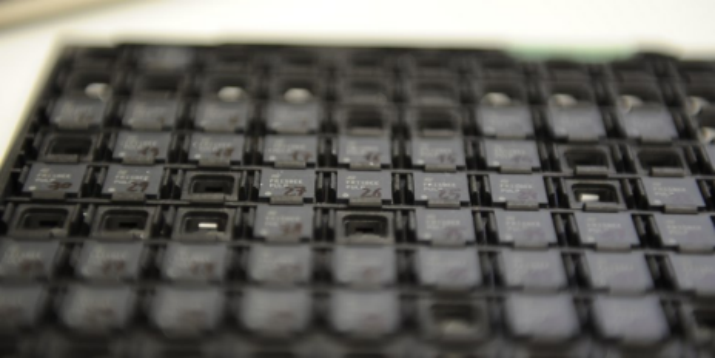 A series of PULP microprocessor chips on a tray. (Image Credit: ETH Zurich / Frank K. Gürkaynak)