Intel has been investing in research at the Cork-based institute since 2009.
Bernie Capraro, Research Manager, Silicon Technology at Intel Ireland, said:
“The standard of work from Tyndall researchers is
top-class, from the work that Dr. Jim Greer does in device modelling to
the photonics work of Brian Corbett. The researchers in Tyndall will be
working directly with Intel’s researchers in Portland, which is the
essence of the programme and what makes it so effective.”
Capraro pointed out that Tyndall researchers bring solutions to Intel – rather than us coming to them with a problem.
Dr. Kieran Drain, CEO of Tyndall National Institute, said:
“Intel has world-class research partners on its doorstep
in the western United States, so the fact that they would come thousands
of miles to work with us here at Tyndall is reflective of our ability
to offer a valuable alternative viewpoint.”
“We have excellent scientists who have a creative approach to future
challenges associated with the extension of Moore’s Law and Intel’s
migration towards a focus on the Internet of Things.”
The current phase of the research partnership between Intel and
Tyndall National Institute will run until 2018, under the direction of
Bernie Capraro, Research Manager, Silicon Technology at Intel Ireland,
and Peter Smyth, Business Development Executive at Tyndall.
Advanced Semiconductor Engineering Inc (ASE, 日月光半導體) yesterday said
negotiations to fully acquire rival Siliconware Precision Industries Co
(SPIL, 矽品精密) remain under way, shrugging off the effects of
macroeconomic uncertainties in the wake of the British decision to leave
the EU.
ASE and SPIL last week extended the Saturday deadline to
sign a joint share-exchange agreement by five days to tomorrow. The
agreement would pave the way for ASE to strike a friendly takeover deal.
ASE,
the world’s biggest chip packager and tester, owns a 25 percent stake
in SPIL and plans to buy the remaining 75 percent for about NT$128.7
billion (US$3.97 billion).
“ASE is in talks with SPIL to sort out
some legal details. We intend to wrap up talks by June 30. We have not
been affected by Brexit at all,” ASE chief operating officer Tien Wu
(吳田玉) told reporters ahead of the company’s annual shareholders’ meeting
yesterday.
“We want [the deal] to create synergies,” Wu added.
When
it comes to mergers and acquisitions, ASE looks at how such deals will
affect the company’s fundamentals for the next 10 to 20 years, while
Britain’s vote to leave EU is not a deciding factor in the company’s
search for merger targets, Wu said.
Wu expects Brexit to hit
global financial markets and foreign exchange markets in the short term,
saying it will not have a contagious effect on consumer confidence, but
added that the consequences of Brexit remain to be seen in the long
run.
ASE and SPIL on May 27 signed a joint share-exchange
memorandum of understanding to push for the creation of an industrial
holding company proposed by ASE. The holding company is to own and
operate both firms.
Based on the memorandum, SPIL is to sell all of its shares to the
holding company at NT$55 per share, while ASE shareholders would be
allowed to exchange their ASE shares for 0.5 shares in the holding
company.
Wu also provided updates on ASE’s business outlook, saying it feels “tight capacity constraints now.”
The
capacity constraints are expected to carry into the third quarter and
ASE plans to add more capacity to cope with growing client demand, Wu
said.
“The second half will be better than the first half... Demand for mobile phones looks very strong,” Wu said.
The growth pattern in the second half will be very similar to that of last year, he added.
Wu
said supply chain inventory has returned to a reasonable level and
excessive inventory will not be an issue this year, adding that instead,
customer demand will be on his radar.
ASE shareholders yesterday
approved a cash dividend of NT$1.6 per common share, based on the
company’s net profit last year of NT$20.3 billion, or earnings per share
of NT$2.55.
The distribution represents an about 4.52 percent dividend yield, based on the stock’s closing price of NT$35.4 yesterday.
nterestingly, this latest 5G prototype system from Qualcomm operates
in the sub-6GHz spectrum bands and not in the millimetre-wave (28-65GHz)
frequency bands.
However, this just confirms the likelihood of a two stage
introduction of 5G services over the next five years or so. First
systems will look a lot like an upgrade of 4G operating in sub-6GHz
bands.
Qualcomm already has a mmWave prototype system for 5G research, operating at 28GHz.
The market may have to wait for the proposed IoT-centric 5G
technology using the millimetre-wave frequencies to meet the expected
data capacity needs. This is now likely to happen sometime after 2020.
According to Qualcomm, utilising spectrum bands below 6GHz for 5G
will be “a critical part of allowing for flexible deployments with
ubiquitous network coverage”.
Qualcomm wants to use the sub-6GHz prototype system “to drive 3GPP standardisation for a new, OFDM-based 5G NR air interface”.
“The prototype system will closely track 3GPP progress to help
achieve timely 5G NR trials with mobile operators, infrastructure
vendors,” said the chipset supplier.
The 5G NR prototype system consists of both a basestation and user
equipment. It supports radio channel bandwidths over 100MHz, and has
lower over-the-air latency than what is possible in today’s 4G LTE
network, says Qualcomm.
Qualcomm is working closely with China Mobile Communications on 5G
technology development to support the work required for 3GPP 5G
standardisation. The prototyping platform is being demonstrated at
Mobile World Congress Shanghai.
The head of the body which represents UK electronic component
distributors and suppliers believes the sector should “keep its heads
down” and try to continue as normal.
“The electronic components supply networks in the UK and
internationally are well positioned to manage a period of turbulence,”
said Fletcher.
“Organisations in our market have long experience in managing large
fluctuations in exchange rates, highly uncertain customer demand
forecasts and today have good inventory availability to support their
customer’s needs.”
Fletcher is hopeful that after the inevitable short term adjustments
as markets react to the actual outcome of the EU referendum and stepping
down of the Prime Minister, “the fundamental underlying economic
position of the UK is not diminished and after a short period of
adjustment it will return to more stable and normal conditions,” said
Fletcher.
On Semiconductor Corp : On semiconductor extends tender offer to
acquire Fairchild Semiconductor . Offer will now expire one minute
following 11:59 p.m., New York city time, on July 7, 2016 .All other
terms and conditions of offer remain unchanged.
IBM is warming up to the idea of adding servers using its Power
processors and the OpenCompute open design to its product portfolio.
"I'm going to bring OpenCompute servers into my portfolio at
some point so that I'm offering directly to the marketplace if there's a
demand for it," said Doug Balog, general manager for Power Systems at
IBM.
An OpenCompute-based Power server will be based on open
designs, and provide an alternative to IBM's integrated systems like
PurePower. It'll also provide customers more flexibility on the
components used inside systems.
A Power-based OpenCompute server
will also be an alternative to open server designs based on x86 chips.
One target for such Power servers is hyperscale vendors, who may be
looking for an alternative to Intel chips, which now dominate data
centers.
Balog didn't say when servers would be added to the Power lineup. But Google and Rackspace are building a server called Zaius based
on IBM's upcoming Power9 chip, which will ultimately be submitted to
OpenCompute. Rackspace in the past developed a Power8 server called Barreleye, and that design was submitted to OpenCompute.
OpenCompute
started in 2011 and provides open server designs. Its members include
Facebook and Google, which are building mega-data centers and largely
designing servers in-house to meet their specific needs. Those servers
are made by companies like Foxconn and Wistron and supplied directly to
the companies. That can be cheaper than buying servers through vendors
like Dell or Hewlett Packard Enterprise.
Most servers that ship
today are based on Intel chips, but IBM believes it has a more powerful
alternative with its Power processors and it has a good fit with
OpenCompute.
"There is no doubt we want Power to be a first-class
member from a processing standpoint as part of the OpenCompute
architecture," Balog said.
More
companies, especially in the financial sector -- which are big
customers of Power servers -- are moving to servers based on OpenCompute
architecture, Balog said.
Three years ago, IBM formed the OpenPower Foundation
-- which boasts members like Google, Samsung, and Nvidia -- to open up
the Power architecture and promote hardware and software development. As
a result, other server makers are offering systems with Power chips.
If
not buying from IBM, companies can also tap into that OpenPower
ecosystem to get servers based on OpenCompute designs, Balog said.
IBM
wants to mainly sell Power servers costing more than US $6,000, while
letting other server makers offer low-end systems. Some of those
vendors, like Tyan, are based in China. Another company offering Power
servers is Supermicro, which has its headquarters in San Jose but has a
big China presence.
Original design manufacturers like Wistron,
which make custom servers based on OpenCompute designs, are also members
of OpenPower Foundation, Balog said.
IBM currently ships servers
based on the Power8 architecture. Servers based on the Power9
architecture are expected to ship in the second half of next year.
Power9 has new features like support for NVLink, a new throughput
mechanism that is five times faster than PCI-Express 3.0.
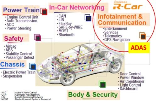
TORONTO—One area where SRAM is seeing some continued stickiness is the growing automotive segment,
as vehicles continue to get smarter and provider more digital
information, whether it's to help the driver or entertain the
passengers.
The segment also includes autonomous vehicles, something Renesas
Electronics Corp. has in mind for its new two-port on-chip SRAM for use
in SoCs for in-vehicle infotainment systems. The new on-chip SRAM will
be used as video processing buffer memory in high-performance SoCs that
will play an important role in making the autonomous-driving vehicles of
the future safer and more reliable.
In a telephone interview from Tokyo with EE Times, Koji Nii, chief
professional for the Design Platform Business Department within Renesas'
1st Solution Business Unit, said the autonomous vehicle market is fast
approaching on the horizon in Japan, as the country has committed to
making it possible for highways to accommodate self-driving cars by
2019, followed by downtown city cores in 2022.
Already, advanced driver assistance systems (ADAS) such as automatic
braking employing radar or other sensors have become widespread, as well
as technology uses video data from vehicle cameras to recognize the
peripheral environment and the driver in order to provide accurate
information to the driver, said Nii. While Renesas supports a number of
electronic systems within vehicles, encompassing MCU and SoC offerings
for power train, chassis, in-car networking, safety and security
applications, the new SRAM is aimed the infotainment and communication
systems of the car, where fast, real-time processing is particularly
important, including video.
A large amount of SRAM configured as high-performance internal buffer
memory is essential for fast and accurate processing of video data. In
addition to increasing the operation speed of the SRAM, said Nii, it's
also critical to enable multi-port operation allowing simultaneous read
and write accesses, which fetch video processing data for operations and
store the data after operations finish.
Renesas has fabricated SRAM prototypes using a 16nm process that
achieved a fast read access time of 313 picoseconds at the low voltage
of 0.8 V. Nii said ingle-port SRAM cells are used to implement two-port
SRAM functionality that allows independent read and write operations,
making it possible to achieve fast read access alongside power
efficiency and compact chip size.
Renesas
supports a number of electronic systems within vehicles, but its new
SRAM is aimed the infotainment and communication systems that require
fast, real-time processing.
This is the third time the company has developed on-chip SRAM with a
16nm FinFET structure. It previously developed an on-chip single-port
SRAM allowing either read or write access at any one time, as well as an
on-chip dual-port SRAM allowing simultaneous read and write operations.
Both have been used in Renesas' R-Car SoCs for in-vehicle infotainment
systems.
The latest SRAM incorporates a double-pumping circuit technology
using single-port SRAM cells, said Nii, which is what allows independent
read and write operations, more compact memory area on the chip while
maintaining fast read access, and reduced power consumption. Related to
the latter is the development of a low-power circuit using a FinFET
structure that effectively reduces leakage power to approximately
one-half the previous level during the standby mode.
Switching from the planar transistor structure used with the earlier
28nm process to a 16nm FinFET structure provides improved transistor
on-off characteristics while also changing the leakage current thermal
characteristics and the voltage dependency. With the 28nm process, it
was possible to reduce leakage current by lowering the voltage, but
FinFET is less voltage-dependent, lowering the voltage did not decrease
the leakage as much as anticipated. Instead, Renesas developed a
low-leakage circuitry that applies bias to the source line potential of
the new SRAM cells that reduces leakage while being relatively
unaffected by thermal characteristics or process corner inconsistency.
In the past, Renesas used dedicated multi-port memory cells while at
the same time developing SRAM for highly accurate and faster video data
processing. But that approach presented challenges with increased
on-chip area and power leakage because more elements were required than
with ordinary single-port memory cells. Renesas developed an SRAM macro
using conventional single-port SRAM cells that implements the
double-pumping circuit technology to enable simultaneous read and write
operations in a single clock cycle.
Renesas recently presented the aspects of its new SRAM technology,
including both the double pumping and low circuit design using FinFET,
at the 2016 Symposia on VLSI Technology and Circuits.
Nii sees a lot of potential in the automotive market to support ADAS
and other infotainment systems with more complex graphics including 3D,
as well as the autonomous vehicle segment.
SRAM is not the only memory that is finding its way into vehicles, of
course. It all depends on the application. For example, when Cypress
acquired Spansion, it also inherited that company's HyperRAM technology,
an alternative to the commonly used options of SRAM or PSRAM. Its fast
read time makes it suitable for automotive applications such as such as
instrument clusters, infotainment and advanced driver assistance
systems.
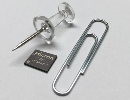
Flash and DRAM also have a role to play in automotive systems. Last
year, Micron debuted its XTRMFlash memory, specifically for applications
that have an “instant on" requirement. The low pin count NOR flash
memory supports human-machine interface with graphical user display,
instrument clusters, infotainment systems and advanced driver assistance
systems (ADAS).
Micron's
XTRMFlash memory is designed for applications that have an “instant on"
requirement, including instrument clusters, infotainment systems and
advanced driver assistance systems (ADAS).
Micron also offers LPDDR4 for the automotive segment as it well suited
to meet overall speed requirements for applications and is able to fit
into the smaller spaces of compact automotive systems. Both NOR flash
and DRAM are being used in dashboard clusters, while eMMC and SSDs are
being used for infotainment data storage.
Although it's primary use is high-end smartphones which require high density yet low power memory to handle 4K video, Samsung's 12Gb LPDDR4 mobile DRAM could
support automotive applications as well, as instrument clusters become
more powerful and require more computational horsepower and more high
quality graphics.
Meanwhile, FRAM is also a candidate for automotive,
as it can be used for nonvolatile data logging in most automotive sub
systems such as smart airbags, stability control, power train, dashboard
instrumentation, battery management, engine controls and infotainment
applications. AEC-Q100 qualified FRAMs are built to bear the extended
grade temperatures under the hood.
Research firm Databeans predicts the
automotive semiconductor market will reach a high of $40 billion in
2020, thanks to the growing amount of electronic content in today's
vehicles such as assisted-driving systems, built-in GPS, satellite radio
menus, vehicle-to-vehicle communications and other infotainment
systems.
Samsung Electronics Co. has officially
announced to reduce its investment in DRAM this year. Until now, there
have been rumors that major semiconductor firms, including Samsung
Electronics, will reduce the DRAM investment. However, it is the first
time for Samsung Electronics to directly reveal its DRAM investment
reduction plans.
According to Samsung Electronics and investment banking industry
sources on June 20, Samsung Electronics held investor relations (IR)
events for institutional investors in the U.S. and Korea last week and
this week.
At the IR event held in New York and Boston from the 14th to 16th
(local time), investors paid attention to 3D NAND flash, organic
light-emitting diode (OLED) and smartphone sales performance. In
particular, Samsung Electronics revealed its plan to reduce the
investment in DRAM at the event for the first time this year.
The company’s NAND flash business is a cash cow which can make up for
sluggish sales in the DRAM sector and boost total sales in the
semiconductor sector. Samsung Electronics significantly increased
margins in the NAND flash sector this year through steady cost
reduction. Its operating margins in the NAND flash sector will grow from
17 percent last year to 25 percent this year.
As global NAND flash manufacturers, such as Intel and SK Hynix, have
recently increased the investment in 3D NAND flash production
facilities, Samsung Electronics is expected to expand the investment in
its production facilities to lose its competitors.
Considering the fact that the NAND flash memory capacity of its new
smartphones to be released in the second half of the year will be
doubled, the construction of its new NAND flash production lines is
inevitable.
Samsung
Electronics is preparing for the winner-take-all system in the NAND
market. The company has the V-NAND flash production lines in Xi'an,
China, and it is considering using the 17th line at the Hwaseong plant
as the 3D NAND-only line. Most industry watchers believe that it will
produce 3D NAND flash chips at its plant in Pyeongtaek, which will start
operation in the middle of next year.
An official from Samsung Electronics said, “We haven’t decided what
to produce at the Pyeongtaek plant yet. Since there is a lot of
volatility in the semiconductor market, we will watch market conditions
until the first half of next year and decide what to manufacture at the
last minute.”
Samsung Electronics ranked top with a 31.6 percent share in the NAND
flash market as of the end of last year, followed by Toshiba with 18.3
percent, SanDisk with 17.6 percent, Micron with 13.4 percent, SK Hynix
with 10.7 percent, Intel with 7.5 percent, Macronix with 0.7 percent and
Powerchip with 0.2 percent. The NAND flash market is relatively crowded
with competitors than the DRAM market.
Samsung Electronics said, “The demand of solid-state drive (SSD) is
increasing, based on 3D NAND flash chips for enterprise (server and
storage). Also, the demand of SSD is rapidly changing as the price
difference with hard disk drive (HDD) is decreasing due to cost
reduction from technology improvement.” Investors had low expectations
for 3D NAND flash until last year but they are welcoming such changes
this year.
In addition, they were interested in OLED investment and flexible
display technology. Lee Sae-chul, an analyst at NH Investment, said,
“Investors expects that smartphones using flexible OLED displays can be a
game changer when they can support tablet functions at the same time.
They had particularly higher expectations for foldable smartphones than
expected.”
As Samsung Electronics seeks to maximize the profitability in the
smartphone market, which has entered the maturity, rather than to expand
its market share, investors in the U.S. positively rated the
performance improvement in the IT and mobile (IM) division.
Meanwhile, Samsung Electronics focused on the next-generation
Internet of Things platform ARTIK, quantum dot and semiconductor
packaging at the IR event for institutional investors held at Conrad
Hotel in Yeouido, Seoul.
In a threat to U.S. technology dominance, the world’s fastest
supercomputer is powered by Chinese-designed semiconductors for the
first time. It’s a breakthrough for China’s attempts to reduce
dependence on imported technology.
The Sunway TaihuLight
supercomputer, located at the state-funded Chinese Supercomputing Center
in Wuxi, Jiangsu province, is more than twice as powerful as the
previous winner, according to TOP500, a research organization that
compiles the rankings twice a year. The machine is powered by a SW26010
processor designed by Shanghai High Performance IC Design Center, TOP500
said Monday.
"It’s not based on an existing architecture. They
built it themselves," said Jack Dongarra, a professor at the University
of Tennessee and creator of the measurement method used by TOP500. "This
is a system that has Chinese processors."
The new machine shows China’s determination
to build its domestic chip industry and replace its dependence on
imports that cost as much as oil. The world’s most populous country may
also try to lessen its reliance on U.S. companies for defense technology
and security infrastructure. Supercomputers aren’t major consumers of
chips. But being at the heart of the world’s most powerful machines
helps processor makers persuade the broader market to consider their
technology."This is the first time that the Chinese have more
systems than the U.S., so that, I think, is a striking accomplishment,"
said Dongarra. The Chinese had no machines in the 2001 list, he noted.
In the latest, China has 167 entries compared with 165 for the U.S.
Previous
supercomputer winners have had processors built on U.S. technology from
Intel Corp. -- the world’s largest chipmaker -- International Business
Machines Corp. or a derivative of Sun Microsystems designs.
The
top position was previously occupied by Tianhe-2, built on Intel chips
by China’s National Supercomputer Center in Guangzhou. That system is
now second, according to TOP500.
Sunway
TaihuLight’s victory is a particular challenge to Intel’s dominance in
computer servers, where it currently controls about 96 percent of the
market. It announced a joint venture with a Chinese organization to
domesticate some of its technology earlier this year.
Supercomputers
are multiple server computers linked together in a way that allows them
to process huge data sets and run the most complex calculations. While
they’re hugely expensive and relatively rare, they showcase new
technologies that often make their way into corporate data centers.
An Intel spokesman declined to comment on the new rankings.
Other
chipmakers such as Qualcomm Inc. are working with Chinese organizations
to build processors in the country. Technology provider ARM Holdings
Plc, whose products are at the heart of most smartphones, is also trying
to grab a slice of the Chinese market.
Jack Ma's comment that fake products made today are "better quality and
better priced" than the real goods should not be taken as a reflection
of the company's failure to curb counterfeits, counterfeit experts said.
The e-commerce CEO made his comments on Tuesday at an investor
meeting in Hangzhou. According to reports, he said the better quality of
the fake goods is due to many of them being made at similar factories,
sometimes with the same labor force using the same materials.
"They are exactly the same factories, exactly the same raw materials
but they do not use the names," Ma said, according to The Wall Street
Journal.
He also said the problem of counterfeit goods cannot be solved "100
percent, because it's the fight against human instinct", according to
The New York Times. "But we can solve the problem better than any
government, than any organization, than [anybody] in the world."
Ma's remarks were made in response to persistent criticism from
luxury brands that the company is not doing enough to get rid of
counterfeit goods on its sprawling e-commerce platform Taobao, where it
is easy to find fake designer bags and jewelry.
Peter Yu, professor of law at Texas A&M University, said in an
interview that counterfeits can be classified into various categories,
with Ma most likely referencing "A-grade" goods that are so difficult to
tell apart that they can only be verified by lab technicians or the
original manufacturer.
"From the perspective of brands, when they see fake goods on Alibaba,
they believe that Alibaba hasn't done enough to enforce and protect
intellectual property rights, and that Alibaba should do more," said Yu,
who is also co-director of the Center for Law and Intellectual Property
at Texas A&M.
"But the part of the story that isn't emphasized is how much money
and effort those auction sites have already put in to police the
networks," he said.
Yu said that fake goods are also available on eBay, Alibaba's
American equivalent, but the scale of counterfeiting in China is much
larger, so even with the resources that Alibaba is putting into combat
the proliferation of fakes, brands might still feel the efforts are
inadequate.
Alibaba had been criticized by the Chinese government for failing to
curb fakes, and late last year the US government issued a stern warning
to the company, saying it could be added back to the "Notorious Markets
List" if it does not do a better job enforcing piracy rules.
Alibaba had been admitted as a general member of the International
AntiCounterfeiting Coalition (IACC), a group that represents many luxury
brands, but the category was suspended a month after it had been
admitted under the new category. The organization's board of directors
said the suspension was due to concerns from members of the group, which
the Journal reported included Michael Kors. A representative from
Michael Kors declined to comment.
"I think the focus of the conversation in the industry isn't to point
fingers at Alibaba or any marketplace, but about making sure that our
technologies are advanced, that they're easy to apply, track and trace,"
said Rich Cremona, CEO of OpSec, a brand protection company whose
clients include other brands in the IACC, of which it is also a member.
Cremona said in an interview that Alibaba works closely with its
clients to ensure that goods are legitimate, and that there has been a
"real effort for many of these online market places to step up
enforcement to define legitimacy".
At the investor meeting, Alibaba forecast that its sales through the
year ending March 2017 will rise at least 48 percent, which is the
company's first financial forecast since the US Securities Exchange
Commissionannounced it was investigating the company's accounting
practices.
ASML Holding NV, one of the biggest producers of chipmaking
equipment, agreed to buy Taiwan-based Hermes Microvision Inc. for about
NT$100 billion ($3.1 billion) to add technology for creating smaller and
more advanced semiconductors.
ASML, based in Veldhoven,
Netherlands, is paying NT$1,410 per share in cash, or 31 percent more
than Hermes Microvision’s average price in the past 30 days, the
companies said in a statement Thursday.
Chip equipment makers are consolidating
to acquire the scale needed to cope with the increasing cost of the
fundamental technology that goes into semiconductors. That also puts
them in a better position to negotiate with the few companies that can
still afford to build leading-edge production facilities. Just three
customers, Intel Corp., Samsung Electronics Co. and Taiwan Semiconductor
Manufacturing Co., account for the majority of spending.
The
Dutch manufacturer is the industry leader in lithography machines that
etch the lines into materials deposited on silicon disks, which create
the tiny circuits that enable chips to process complex computations. For
most of the past decade, ASML has been touting extreme ultraviolet lithography systems,
which can produce smaller chips while increasing capacity and speed.
Hermes Microvision’s equipment checks that steps in the manufacturing
have been properly completed.Unlike some more recent deals in
semiconductor production equipment, which focused on cost synergies, the
acquisition of Hermes Microvision is about technology, Morgan Stanley
analysts said in a note to clients.
“We believe this is a strong
sign of confidence in the future of EUV and we still expect good news on
the order side in the next several months,” they said.
Hermes
Microvision shares climbed 9.9 percent in Taipei, hitting the daily
limit. Shares of Nikon Corp., which competes with ASML, ended the day
2.8 percent lower at 1,408 yen in Tokyo. ASML shares were up 0.2 percent
to 84.07 euros at 4 p.m. in Amsterdam.
ASML
is financing its purchase with cash, about 1.5 billion euros ($1.7
billion) of debt and 500 million euros of ASML stock that will be bought
by Hermes Microvision’s main shareholder and the Taiwanese company’s
executives. Part of the proceeds will be reinvested in Hermes
Microvision, and ASML said the deal will immediately add to its
per-share earnings.
The price tag isn’t too high as Hermes
Microvision isn’t yet fully mature, Edwin de Jong, an analyst for SNS
Securities, said in a note to clients. Hermes’s technology adds value to
ASML’s existing products, adds yield through a new machine and its
management is participating by buying ASML stock, he said.
“Financially, HMI is extremely profitable and will add value to ASML shareholders within a couple of years,” he said.
While
the companies have worked together for almost two years, ASML started
negotiations to acquire the Taiwanese firm toward the end of last year,
according to a person familiar with the matter. Goldman Sachs Group Inc.
advised Hermes Microvision, while ASML was working with Credit Suisse
Group AG, two people said, asking not to be identified as the
information is private.
A representative for ASML declined to
comment beyond the company’s statement, while a spokesman for Hermes
Microvision didn’t answer three calls to his office seeking comment. A
spokeswoman for Credit Suisse didn’t answer calls seeking comment, while
a representative for Goldman Sachs declined to comment.
In
the next 10 years, the medical technology industry is projected to
shift from systems dependent on CRTs to those reliant on LCDs. Although
there are a host of foreseeable benefits to the technological
advancement, it also poses a serious concern: Will existing modalities
have to be replaced in order to be LCD compatible?
As an alternative to the purchase of entirely new systems, Ampronix
has introduced Modalixx, an LCD display system compatible with Cath Lab,
MRI, CT, RF rooms, Mobile C-Arm, computed radiography, PET scanner, and
nuclear medicine modalities. In addition, the company says Modalixx is
relatively low-cost with a long life span, requiring fewer repairs than
CRTs.
A shift from CRT to LCD medical technology is likely within 10 years. (Credit: Ampronix)
Switching
over from CRT to LCD would offer brighter resolutions, lower power
consumption and no radiation emissions. The company says it can replace
all types of modality CRT's, sync to an existing technology set-up,
and can receive any video signal parameters. Compatible systems include
Eizo, GE, Phillips, Siemens and Toshiba, among others.
With inputs ranging from one to five BNCs and 15 pin D-Sub
connectors, a range of analog connectivity is provided. The technology
allows Modalixx to convert small matrix pictures from analog to two
megapixel images, thus converting medical renderings without
compromising the integrity of images, allowing medical professionals to
zoom-in or zoom-out at their choosing.
Without set universal standards for medical grade displays, the
responsibility falls largely on individual companies to upgrade
technology as needed to provide optimized care, according to the
company.
DRAM chipmaker Inotera Memories Inc (華亞科技) yesterday said Micron
Technology Inc is proceeding with its purchase of the remaining
67-percent share of Inotera, defusing investor concern that the NT$130
billion (US$4.01 billion) acquisition deal was collapsing.
“We are
optimistic about closing this deal,” Inotera chairman Lee Pei-ing (李培瑛)
told a media briefing. “We will assist Inotera and other agencies to
complete the transaction.”
Lee also serves as president of local
DRAM chipmaker Nanya Technology Corp (南亞科技), which is in talks with
Micron to sell its 24 percent share of Inotera, as well as
next-generation technology transfer from the US memorychip giant.
Inotera
shares took a 9.86-percent nosedive yesterday after Micron said it
would postpone its purchase of remaining 67 percent stake in its
Taiwanese DRAM arm from Nanya and subsidiaries of Formosa Group (台塑集團).
Micron originally expected the deal to close in the middle of next month.
The
“parties have concluded that closing the transaction on this timeframe
is not possible,” Micron said in a statement on Thursday.
The Boise, Idaho-based memorychip maker said it “expects to provide an update toward the latter part of calendar 2016.”
“There
are some procedures that needed to be taken care of. Inotera and Nanya
are working on these procedures,” Inotera spokesman Peter Shen (沈道邦)
told reporters.
The company is working smoothly with banks to
arrange NT$80 billion in syndicated loans to facilitate the share
purchase, Shen said.
“This is not the factor that is causing the delay,” he said.
Micron
subsidiaries currently hold about 33 percent of the issued and
outstanding shares of Inotera. In December, Micron offered NT$30 per
common share to acquire all of the issued and outstanding shares of
Inotera via its local unit, Micron Semiconductor Taiwan Co (台灣美光).
The stock price of Inotera plunged to NT$26.5 and retained at the
level through the whole trading session yesterday after the local bourse
resumed trading after four-day Dragon Boat Festival holidays.
“Judging
from the selling in Inotera shares, I think many investors are not
satisfied by the clarification from Inotera. The market needs more
information about the acquisition deal, so for the moment, investors
rushed to dump Inotera shares,” Mega International Investment Services
Corp (兆豐證券) analyst Alex Huang (黃國偉) said.
“The acquisition price
served as an anchor to stabilize Inotera shares in recent sessions. Now,
how the deal will proceed is being questioned, and investors simply
locked in their earlier gains today, and a bigger downturn is possible,”
Huang said.
Additional reporting by CNA
Apple will use Intel chips over Qualcomm's for some versions of the iPhone 7, Bloomberg reports. The development would be significant for Intel, which has seen serious setbacks in its mobile ambitions this year.
Intel said it does not comment on rumors, while Apple did not immediately respond to a request for comment.
Apple
is turning to Intel modem chips for versions of the iPhone used on
AT&T's U.S. network and some used in overseas markets in an effort
to diversify its supplier base, Bloomberg reports, citing unnamed
sources familiar with the matter. Apple will reportedly still use
Qualcomm chips for phones on the Verizon network and iPhones sold in
China.
When Intel CEO Brian Krzanich took the helm of the company in 2013, he emphasized Intel's focus on the mobile market, and over the past three years the company spent more than $10B to gain a foothold in mobile. In April of this year, Intel announced it was hiring Dr. Venkata "Murthy" Renduchintala from Qualcomm, which would seemingly help its mobile prospects. Yet just weeks later, Intel announced it was canceling upcoming Atom smartphone chips code-named Broxton and Sofia, a move that was seen as effectively giving up on the smartphone market.
For Apple, diversifying its suppliers for the iPhone, which brings in the bulk of its revenue, is a clearly smart business move.
As
Intel shifts its strategy to become more of a cloud, data center and
connectivity source, partners play a more important role now than ever,
channel executive Maurits Tichelman told CRN on Thursday.
"Intel remains … extremely committed and continues to invest in the
channel," said Tichelman, the vice president who oversees Intel's
channel sales and marketing. "There should be absolutely no confusion in
terms of Intel’s strategy going forward. The role of the channel to me
and to Intel is more important going forward than looking backward."
Tichelman laid out what he said were those potential opportunities
involving partners: "Looking at IoT and data center, there are many more
new business models being developed where Intel technology can be at
the core and heart of solutions," he said, "but we want to make sure
that our channel stays close to us so we can learn from our channel and
can keep developing great products, not only for today but for the
future."
CEO Brian Krzanich in April said the data center and the Internet of
Things would be the Santa Clara, Calif.-based company's future as it
aims to lessen dependence on the PC market, to "create lasting value for
our customers, partners and shareholders, and achieve our mission to
lead in a smart, connected world."
The shift in strategy is in part because of a stagnant PC market:
Intel last quarter lowered its PC market expectations, saying it expects
the market to decline in the high single digits in 2016 -- more than
earlier expectations.
Meanwhile, the company's data center segment, which grew 9 percent
year over year in the first quarter, as well as its Internet of Things
segment, which grew 22 percent year over year, are lucrative markets.
Tichelman said Intel's focus on these areas can only be positive for
the channel, as many partners have already undergone a "natural
evolution" into embedded compute areas and cloud computing capabilities
that power IoT and the data center.
"To me, this is encouraging to us as a channel organization that this
strategy will potentially boost and demonstrate the potential of the
channel," he said. "We have seen many partners evolving in looking at
what else they can do with the IT knowledge that they have. We've seen a
natural evolution of many of our customers' expanding their
capabilities and going into embedded compute areas, and embedded compute
to IoT is a very natural evolution."
The partner interest in lucrative IoT and data centers is prevalent
-- according to an Intel survey, more than 70 percent of Intel's
partners are offering managed services, which Tichelman said is "one key
indicator that strengthens the belief that the channel is essential to
the overall data center build-out."
The study also revealed that more than 65 percent of partners are
offering cloud capabilities to their customers. And out of Intel’s
150,000-strong partner base, the study said, 25,000 partners stated that
they are already involved in some way in the IoT business.
Going
forward in 2016, Tichelman said, Intel will continue to help partners
pinpoint opportunities for profit in the data center and IoT segments.
For instance, Intel will continue its rollout of high-performance
computing (HPC) and cloud specialty benefits, which give recognition to
and reward partners that meet certain requirements in those segments, as
well as make sure it is "activating" partners with Intel-based
technology in the IoT space.
Martin Smekal, president and CEO of Torrance, Calif.-based Intel
partner TabletKiosk, said he feels "cautiously optimistic" about Intel's
future as a cloud and data center source, and what that implies for the
channel.
"Brian Krzanich has made the right move, and I agree with his
direction," said Smekal. "The cloud is huge. ... You need data center to
back cloud, and that involves service centers, areas where we can make
margin in the channel. I also like the fact that he's focusing on IoT.
It's slow and it's still developing, but overall, it's a positive as a
whole for the channel."
SAN FRANCISCO—U.S. memory chip maker Micron
Technology Inc. said Wednesday (June 8) the timeframe for its
acquisition of Inotera Memories Inc. has been pushed back beyond the
original target date of next month.
Micron’s $4 billion deal to buyout partner Nanya Technology Corp. and
take 100% control of the Taiwanese DRAM joint venture was initially
expected to close in mid July. But Micron (Boise, Idaho) said Wednesday
that the two parties have concluded that closing the transaction on this
timeframe is not possible.
Micron announced in late 2015
it would acquire Nanya’s roughly two-thirds stake in Inotera in a cash
and stock deal worth about $4 billion. Micron already owns about 33% of
Inotera and buys 100% of the JV’s DRAM production.
Micron declined to provide more information about what is holding up the deal.
DRAM pricing has been under pressure for more than a year. First
quarter DRAM sales declined 16.6% compared with the fourth quarter of
2015, due mainly to oversupply and declining average selling prices,
according to the DRAMeXchange, a unit of market research firm
TrendForce.
Micron said it would provide an update on the acquisition later this year.
PASADENA, Calif. — The future of computing may be in its past.
The
silicon transistor, the tiny switch that is the building block of
modern microelectronics, replaced the vacuum tube in many consumer
products in the 1970s. Now as shrinking transistors to even more
Lilliputian dimensions is becoming vastly more challenging, the vacuum
tube may be on the verge of a comeback.
In
a darkened laboratory here, two stories beneath the California
Institute of Technology campus, two students stare through the walls of a
thick plastic vacuum chamber at what they hope will be the next small
thing — a computer chip made from circuits like vacuum tubes whose
dimensions are each roughly one-thousandth the size of a red blood cell.
At
stake is the future of what electronic engineers call scaling, the
ability to continue to shrink the size of electronic circuits, which is
becoming harder to do as they become as small as viruses.
It
has been more than half a century since the physicist Richard Feynman
predicted the rise of microelectronics, noting “there’s plenty of room
at the bottom.” He used the phrase in 1959 when he speculated about
engineering with individual atoms. Several years later, Gordon Moore,
co-founder of Intel, wrote that the number of transistors that could be
etched into silicon wafers would double at regular intervals for the
foreseeable future.
Now, however, there is growing evidence that space, if still available, is increasingly at a premium.
Progress is slowing down. The time between each new chip generation is
stretching out, and the cost of individual transistors, although
infinitesimal, is no longer falling. The tiny transistors also bedevil
chip designers because as they get smaller, they generate unwanted heat.
For Axel Scherer, who heads the Nanofabrication Group
at Caltech, that means going back to the future. With his students Max
Jones and Daniil Lukin, he is pursuing what is in effect an ultrasmall
vacuum tube as a candidate to replace the transistor. In their
laboratory here, they have fabricated circuits that function like vacuum
tubes but are a millionth the size of that 100-year-old technology.
“Computer technologies seem to work in cycles,” said Alan Huang, a former electrical engineer for Bell Laboratories. “Some of the same algorithms that were developed for the last generation can sometimes be used for the next generation.”
The
last time researchers explored vacuum tubes was in the 1990s, when they
were a promising option for building flat-panel displays. The
technology failed to take off, however, because of cheaper and more
efficient liquid crystal displays.
“The vacuum tube comes back about every decade,” Dr. Scherer said with a laugh.
And
for decades, that has been the story of vacuum tubes: There has always
been a better option. Transistors replaced vacuum tubes because they
were more compact, did not generate skin-burning heat and did not need a
vacuum — the absence of atmosphere made it possible for electrons to
jump between positively and negatively charged elements.
The
vacuum tubes the Caltech researchers are looking at are nothing like
the bulky objects that hummed in the old family radio and even early
computers. Both transistors and vacuum tubes — the British called the
devices valves — control the flow of electricity, but they do so
differently.
The
researchers have created a tiny tube formed from metal and capable of
turning on and off the flow of electrons between four even smaller
probes, which under an electron microscope appear like the tips of four
ballpoint pens almost touching one another.
The
Achilles’ heel of today’s transistors is the smaller they get, the more
they leak electrons. In modern computer chips, as much as half of the
power consumed is lost to electrons leaking from transistors that are
only dozens of atoms wide. Those electrons waste energy and generate
heat.
In
contrast, Dr. Scherer’s miniature vacuum tube switches perform a
jujitsu move by using the same mechanism that causes leakage in
transistors — known by physicists as quantum tunneling — to switch on
and off the flow of electrons without leakage. As a result, he believes
that modern vacuum tube circuits have the potential to use less power
and work faster than today’s transistor-based chips.
“Effects
that are currently problems in scaling are precisely those that we
would like to use for switching in these next-generation devices,” Dr.
Scherer said, noting that while there are efforts to redesign
semiconductor-based transistors around the tunneling effect, his
approach is significantly simpler.
Vacuum
tubes are one of a range of ideas that engineers are looking at as they
work to create chips that can do more while using less power. Other
promising approaches include exotic materials such as carbon nanotubes
and even microscopic mechanical switches that can be opened and closed
just like an electronic gate.
The
Caltech researchers returned to the idea of vacuum tubes several years
ago after they had begun experimenting with the idea of making
ultrasmall incandescent light bulbs no larger than a modern transistor
that would be bright enough to be seen by the naked eye from across a
room.
The
group previously worked in research areas like quantum dots, nanoscale
structures now used in television displays to produce precise colors,
and optoelectronics, a field that explores the use of lasers in
electronic circuits. But they decided to look for new research areas
that were less crowded with competitors.
Today,
semiconductor companies like Intel are making silicon chips with
minimum dimensions between 10 and 20 nanometers. (A strand of DNA is
roughly 2.5 nanometers in diameter.) Once the industry shrinks below 10
nanometers, Dr. Scherer expects that researchers will be surprised by
the behavior of silicon at such atomic dimensions.
For
one thing, silicon emits light below 10 nanometers, he said. More
significantly, it also becomes remarkably elastic as it becomes that
small.
“It’s
a different material, and it gives you this different behavior,” he
said. He sees the future in other materials and in old ideas that would
be made new again.
In
contrast to silicon, a semiconductor, which can either conduct or
insulate, depending on how it is chemically modified, Dr. Scherer’s
tubes can be made from a range of conducting metals, such as tungsten,
molybdenum, gold and platinum. This will be an advantage because it will
significantly simplify the tiny switches at the atomic scale.
Dr.
Scherer does not think the tiny tube will immediately replace the
transistor, but the possibility of applications in space and aviation
has caught the attention of Boeing, which is financing the research. Such specialty chips might be ready commercially before the end of the decade.
“Ten years ago, silicon transistors could meet all of our demands,” he said. “In the next decade, that will no longer be true.”
From PCs to servers, Intel is trying to redesign the way computers
operate. We've already seen how PCs are changing, with 2-in-1 hybrids
and tiny Compute Sticks, but some of the chip maker's groundbreaking
technologies will initially appear in servers.
The PC market is in decline, and the chipmaker has cut
unprofitable products like smartphone chips. Intel is redirecting more
resources to develop server and data-center products, which are already
money makers for the company.
Intel is also focusing on markets
like the Internet of Things, memory, silicon photonics, and FPGAs (field
programmable gate arrays), all of which have ties to the fast-growing
data center business.
Intel
has cut about 12,000 jobs in the transition away from smartphone chips
and PCs. Employees have bought into the company's new strategy, Intel
CEO Brian Krzanich said during a speech at the Bernstein Strategic
Decisions Conference last week.
Many
innovations and "dramatic changes" are coming over the next two to
three years, especially on the data-center side of the business,
Krzanich said.
Intel has always looked at ways to drive up
performance in individual systems, but the company's focus is changing
to drive improvements in server, memory, networking, and storage
components at the rack level. The company is also working to speed up communications between the components.
"We have a lot of good work to do," Krzanich said.
Intel
has pushed a concept called the Rack Scale architecture, which is meant
to bring configuration flexibility and power efficiency to server
installations. The idea is to decouple processing, memory, and storage
into separate boxes on a rack. More memory, storage, and processing
resources can be installed at the rack-level than on individual servers
patched together, and shared resources like cooling could help cut
data-center costs.
Intel's
OmniPath fabric, a superfast interconnect technology, is viewed by
Krzanich as the centerpiece of new server technologies. It will provide
the protocols for CPUs to communicate at faster speeds with components
inside a server and at the rack level. In the future, Intel envisions
data transfers happening over beams of light, which will speed up
OmniPath.
OmniPath will accelerate workloads like analytics and
databases. It will be available through network controllers on Intel's
upcoming Xeon Phi supercomputing chip code-named Knights Landing, but
the ultimate goal is to bring the interconnect closer to the CPU.
"There
are workloads that can be taken from software that's working in memory
to software that's working right on the silicon, right next to the CPU,
with a direct link through the OmniPath fabric," Krzanich said.
Using
beams of light for speedy data transfers is the idea behind silicon
photonics, another technology that's a priority for Intel. Silicon
photonics will replace traditional copper wires, and bring faster data
transfers across storage, processing, and memory components on racks,
Krzanich said.
After delays, Intel has said it will ship modules to implement silicon photonics later this year.
Xeon chips will always be important to Intel, but the chipmaker
is also looking at speedy co-processors called FPGAs to quickly perform
specific tasks. Intel believes a killer combination of CPUs and FPGAs,
which can be easily reprogrammed, could speed up a wide range of
workloads.
FPGAs are already being used by Microsoft to speed up
the delivery of Bing search results, and by Baidu for faster image
search. Intel believes FPGAs are relevant for artificial intelligence
and machine learning tasks. Intel also plans to use FPGAs in cars,
robots, drones, and IoT devices.
Intel acquired FPGA technology
through the US$16.7 billion purchase of Altera last year. The company's
next step is to pack an FPGA alongside its Xeon E5-2600 v4 server
processor on a modular chip. Ultimately, FPGAs will be integrated on
server chips, though Intel hasn't provided a timeline.
Intel is
also developing a new type of storage and memory called 3D Xpoint, which
the chipmaker claims is 10 times denser than DRAM, and 1,000 times
faster and more durable than flash storage. Krzanich described 3D Xpoint
as being a "hybrid between memory and storage." The technology will
first come to gaming PCs under Optane-branded SSDs, but will branch out
to servers in the form of flash storage and DRAM modules.
The
emerging technologies from Intel may require companies to change their
server architectures from top to bottom. But as long as the servers
deliver cost-performance benefits, the technologies will be adopted,
Krzanich said.
Intel hasn't yet provided a cost estimate for the
investment, and it hasn't described how racks infused with new
technologies could be implemented alongside existing server
installations. Intel will continue selling regular server CPUs, but it
may take time for customers to adopt the new technologies until they are
proven.
Intel held a 99.2 market share for server processors in
2015, but that may fall next year as AMD releases new server chips and
the adoption of ARM servers potentially grows.
A new company launched Monday by former NASA chief Dan Goldin aims to deliver a major boost to the field of neural computing. KnuEdge's debut comes after 10
years in stealth; formerly it was called Intellisis. Now, along with
its launch, it's introducing two products focused on neural computing:
KnuVerse, software that focuses on military-grade voice recognition and
authentication, and KnuPath, a processor designed to offer a new
architecture for neural computing.
"While at NASA I became fascinated with biology," said Goldin in an
interview last week. "When the time came to leave NASA, I decided the
future of technology would be in machine intelligence, and I felt a
major thrust had to come from inspiration from the mammalian brain."
Goldin's startup began by focusing on speech recognition in the presence of noise. KnuEdge's technology, which has
already been tested under military conditions, makes it possible to
authenticate a person's voice for computers, Web and mobile apps, and
IoT devices with only a few words spoken into a microphone in any
language and in real-world noisy conditions, the company said. Potential
applications span industries such as banking, entertainment and
hospitality.
"We don't care if you have a cheap or expensive microphone," he said.
"It can go on anyone's computational platform, and we're beginning to
approach error rates measured in parts per billion."
Whereas most work in neural networks focuses on information
structures known as "dense" matrices, KnuEdge tapped "sparse" matrices
instead, Goldin said.
"As far as we know, the sparse matrix in the human brain is the most
efficient," he said. "We used that as a model. We felt it was important
to build a model that replicated how the brain works." KnuEdge's KnuPath LambdaFabric processor technology, meanwhile, was
inspired by a roadblock the company encountered while working on its
voice recognition offering. Essentially, the company realized it could
not achieve the performance it needed with traditional CPUs and GPUs, it
said, so it created a new team to build an application-specific
integrated circuit (ASIC).
KnuPath processors are low-wattage, 256-core chips with 16
bidirectional I/O paths, the company said. With the ability to scale up
to 512,000 devices, they offer rack-to-rack latency of just 400
nanoseconds.
"Each core can run a different calculation simultaneously," Goldin said.
KnuPath can operate alone or be integrated with other devices.
Potential applications include signal processing and machine learning
for the Internet of Things (IoT).
Production platforms and systems will be available in the second half
of this year. KnuEdge plans to make its application programming
interfaces (APIs) available worldwide on a freemium model.
So far, KnuEdge claims private funding totaling US$100 million and $20 million in revenue.
KnuVerse differs from Siri or Google Now in that it focuses on
improving audio quality to the point where it can be used for secure
recognition of an individual in any environment, said Jim McGregor,
principal analyst with Tirias Research.
"Think of it as a version of Google Now on steroids that has been proven by the U.S. government and military," McGregor said.
KnuPath, on the other hand, is "essentially a new processing
architecture designed around creating intelligence from massive amounts
of data, or what is typically called deep learning," he said. "This is a
move away from the CPU paradigm to a entirely new form of computing."
The most obvious competitor in that space today is IBM, but there are
other companies developing neural network technology as well, McGregor
noted. "Look for a wave of innovation in this area over the next few
years."
Together, KnuEdge's technologies could help create smart cities, he
added. While many details remain to be revealed, "seeing new technology
like this makes it an exciting time to be in the industry."
FORT COLLINS – Shares of semiconductor giant Broadcom
Ltd., which has a major presence in Fort Collins, jumped more than 6
percent in after-hours trading Thursday following the company’s first
earnings report reflecting the merger of Avago Technologies and
Broadcom.
San Jose, Calif.-based Avago closed its $37 billion acquisition of
rival Broadcom Corp. in February, with the new company taking on the
Broadcom Ltd. name and trading on the Nasdaq stock exchange under the
ticker symbol AVGO.
The new Broadcom – which at the time the merger closed employed
roughly 1,600 people between facilities in Fort Collins and Longmont,
mostly in Fort Collins – beat analyst estimates for both revenue and
earnings for the company’s second fiscal quarter that ended May 1. The
company also announced that it plans to pay an interim quarterly
dividend of 50 cents per share on June 30 to shareholders of record as
of June 17.
Broadcom posted a net loss of $1.2 billion, or $3.02 per diluted
share, for its second quarter. That’s compared to net income of $377
million, or $1.30 per diluted share for the company’s previous quarter,
prior to combining results for Avago and Broadcom Corp. Revenue grew to
$3.54 billion, double from the previous quarter.
The company also reported a cash balance of $2.04 billion as of May
1. Guidance for the third quarter includes roughly $3.74 billion in
revenue and capital expenditures of about $230 million.
Broadcom shares rose 14 cents Thursday to close at $154.91 before spiking to $164.50 after hours following the earnings news.
In
the 3D NAND flash market led by Samsung Electronics, the alliance
between Intel and Micron is emerging as strong competitors against
Samsung Electronics.
According to market research firm DRAMeXchange on May 30, Intel and
Micron started mass production of 3D NAND flash products at the
Singapore plant in the first quarter this year. They can produce only
3,000 semiconductor wafers per month at the moment, but the production
capacity will skyrocket to 40,000 within the year. Once the Dalian plant
in China starts full-scale operation at the end of the year, their 3D
NAND production capacity will surpass that of Samsung Electronics.
It corresponds with the semiconductor industry’s analysis that 3D
NAND manufacturing technology of Intel and Micron are stabilizing faster
than expected.
Since
Samsung Electronics has practically decided not to make the second
stage of 3D NAND flash investment in the Xi’an plant as the industry
expected earlier, its 3D NAND average production capacity per month will
be around 20,000 to 40,000, said DRAMeXchange. The figure accounts for 9
to 18 percent of Samsung Electronics’ total NAND flash production.
Starting with Intel and Micron, on the other hand, its competitors,
including Toshiba and SK Hynix, are beefing up their production
capacities. So, the experts’ analysis that Samsung Electronics’ 3D NAND
production technology is over three years ahead of other memory
manufacturers is now meaningless.
SK Hynix, which began the 3D NAND shipment in the second quarter this
year, will significantly increase its output in the second half of the
year. The company currently produces 2,000 sheets on a monthly basis but
it plans to raise its production capacity by 10 times to 20,000 wafer
sheets in the fourth quarter.
On the other hand, some industry watchers say that Samsung
Electronics is focusing on improving its mass productivity, rather than
building additional production facilities, in order to brace for 3D NAND
“chicken game” which will be accelerated from next year. In particular,
the company is expected to aggressively establish production lines next
year when the production cost of 3D NAND products will be lower than
that of 2D NAND products.
- See more at:
http://www.businesskorea.co.kr/english/news/industry/14848-3d-nand-competition-intel-micron-threatens-samsung-3d-nand-market#sthash.efTZD5nI.dpuf
In the 3D NAND
flash market led by Samsung Electronics, the alliance between Intel and Micron
is emerging as strong competitors against Samsung Electronics.
According to market research firm DRAMeXchange on May 30, Intel and Micron
started mass production of 3D NAND flash products at the Singapore plant in the
first quarter this year. They can produce only 3,000 semiconductor wafers per
month at the moment, but the production capacity will skyrocket to 40,000
within the year. Once the Dalian plant in China starts full-scale operation at
the end of the year, their 3D NAND production capacity will surpass that of
Samsung Electronics.
It corresponds with the semiconductor industry’s analysis that 3D NAND
manufacturing technology of Intel and Micron are stabilizing faster than
expected.
Since Samsung Electronics has practically decided not to make the second
stage of 3D NAND flash investment in the Xi’an plant as the industry expected
earlier, its 3D NAND average production capacity per month will be around
20,000 to 40,000, said DRAMeXchange. The figure accounts for 9 to 18 percent of
Samsung Electronics’ total NAND flash production.
Starting with Intel and Micron, on the other hand, its competitors,
including Toshiba and SK Hynix, are beefing up their production capacities. So,
the experts’ analysis that Samsung Electronics’ 3D NAND production technology
is over three years ahead of other memory manufacturers is now meaningless.
SK Hynix, which began the 3D NAND shipment in the second quarter this year,
will significantly increase its output in the second half of the year. The
company currently produces 2,000 sheets on a monthly basis but it plans to
raise its production capacity by 10 times to 20,000 wafer sheets in the fourth
quarter.
On the other hand, some industry watchers say that Samsung Electronics is
focusing on improving its mass productivity, rather than building additional
production facilities, in order to brace for 3D NAND “chicken game” which will
be accelerated from next year. In particular, the company is expected to
aggressively establish production lines next year when the production cost of
3D NAND products will be lower than that of 2D NAND products.