Friday, October 30, 2015

Culture Clash In Analog

Different design perspectives begin creeping into analog world as systems engineers enter the market with big-picture ideas and training.
popularity
The analog/mixed signal world is being shaken up by a mix of new tools, an influx of younger engineers with new and broader approaches, and an emphasis on changing methodologies to improve time to market.
Analog and digital engineers have never quite seen eye-to-eye. Analog teams leverage techniques that have been around, in some cases, for decades, while digital teams rely heavily on the latest technology available. While they have co-existed in mixed-signal environments, they have largely gone about their jobs independently.
That is changing as a new generation of engineers enter the market, offering new approaches to design and creating disruptions within semiconductors and tool providers alike.
“It’s the changing of the guard of the people who are designing electronics,” said Darrell Teegarden, mechatronics project manager in the SLE systemvision.com team at Mentor Graphics. He said there is a step-function changing happening now as a number of changes converge on design teams.
“Engineers graduating today are a different breed than when we graduated,” Teegarden said. “What they expect, the way they work — all of these things are very very different, and that’s changing a lot of the dynamics both of the tool companies but also maybe more importantly for semiconductor companies. They have to be system engineers. The courses they are taking [in college] now are holistic. You don’t just focus on transistor design. The senior projects they are doing are entire systems of hardware and software and sensors and actuators. It’s stuff that connects with the Internet. They want to make self-driving cars as a senior project. Their ambitions are almost as ridiculous. They plot these amazing things because they don’t know any better and they have expectations to go with that. It’s that design perspective of whole systems, and then it’s also the expectation of how the world works, like stuff should be free. This is a challenge for companies. But that’s part of the disruption, and with disruption comes opportunity.”
To understand where this is headed, and how it impacts analog modeling, it helps to look at where analog modeling is today.
“If you talk in the context of pure analog Verification, analog modeling refers very often to Verilog-A, where engineers aimed to create a model for an analog block that could describe the behavior of this block and some of its non-linear effects,” said Helene Thibieroz, senior staff marketing manager at Synopsys. “That was strictly for analog or RF — in the context of analog verification—and not meant for mixed signal.”
Some engineering teams have taken system-level approaches doing co-simulation with Matlab to try to do some higher level of modeling, she explained. “If you now extend the concept of analog modeling to mixed-signal, where you have a need to create a behavioral model for speed and accuracy, different standards were created. The first one was Verilog-AMS, which is a language including a mix of constructs from analog and digital. This approach was first primarily used by analog designers aiming to extend their flow to mixed-signal.”
The problem is that, unlike digital tools and standards, analog has never been scalable. Thibieroz explained, “As the Verilog-AMS model is parsed by a mixed-signal simulator, the design code is split internally into a digital portion to be handled by a digital event-driven simulator, and an analog portion to be handled by an analog circuit simulator. The result is typically performance speed-up with reasonable accuracy. Verilog-AMS has, however, several limitations that have made adoption of this language challenging, especially for modern SoCs: it is hard to scale as you need both expertise and model calibration, you need people’s expertise to create those models (someone understanding both analog and digital languages as well as the block behavior they are trying to model) and you need to calibrate those models versus their SPICE counterparts for each process or technology change.”
Real Number Modeling provided the second generation of behavioral modeling where digital simulators model the analog behavior in the digital domain using discretely simulated real values. The end result is a considerable speed-up, but lower accuracy. “For example,” she said, “Real Number Modeling does not accurately represent models having significant feedback loops. As a result, this approach has been adopted for functional verification only but not for modeling high-precision analog blocks. Real Number Modeling also has some existing languages limitations, mostly the lack of support for user-defined types that can hold one or more real and user-defined resolution functions, and no true relationship between current and voltage. So to remove those limitations, a new modeling approach, System Verilog nettype was created: it provides the required enhancements for modern mixed-signal SoC verification (for example user-defined types that can hold one or more real values) so provides the same performance gain with more accuracy. However for all of those models, there is still a crucial need to validate those models versus their SPICE counterparts.”
For this reason, it often becomes challenging for digital verification teams to just rely on those analog models while doing verification. Interactions between analog and digital have become more and more complex and a behavioral model may not be able to fully represent the true interaction of the analog block with the rest of the design at the SoC level.
Depending of the design application and the need for accuracy, Real Number Models may be able to be relied on, or certain blocks may need to be included as SPICE blocks, Thibieroz pointed out. She pointed to certain users that employ only real number models for their analog blocks as the complexity of their analog block is minimal and their transfer functions fairly linear. “For critical blocks that need SPICE accuracy or relate to power management, other users choose not to use analog models but simulate directly with the SPICE analog blocks to get the true behavior of the circuit and therefore fully capture any interaction between analog and digital.”
Those analog blocks are then integrated in the digital verification methodology using technology that allows the designer to extend digital concepts such as assertions and checkers to analog — resulting in a true mixed-signal verification where both digital and analog are being verified simultaneously. In this vein, Qualcomm will present a flow they developed using VCS AMS at the AMS SIG event in Austin next week.
The value of languages
Still, Teegarden has a high level of confidence in modeling languages. “Today, you have ubiquitous kinds of SPICE variants that have all of the advancements in technologies that were available in the early ’70s, and amazingly there is still a lot you can do with SPICE. But we are way past that limitation and the requirements are much greater than that now. The modeling languages are a big help for that. These languages have been around for a while and they are just finally delivering.”
But it also requires a lot of effort to use them effectively. “If you see what people actually do right now, on the IC design side people who do IC design, it’s not that VHDL-AMS or Verilog-AMS have really run out of steam,” he said. “It’s that the natural inclination is to say, ‘If I’m going to model a combination of SPICE level and HDL and RT level – people just don’t use those languages in between because that’s a lot of work. It’s not because the languages are not up to it that they don’t do that work. It’s because it’s a lot of work. You’d rather just throw hardware and time and model the transistor level in SPICE, model the digital stuff at the RT level, and then mash it together. So the languages have been there. They just haven’t been used because of those issues.”
On the developer side, people that are trying to make use of the stuff — that’s where the sweet spot is for these languages, Teegarden suggested. “For one, the IC guys don’t want to put the transistor-level IP out in a model on the Internet. That’s not a good idea. And even if you did, it’s too slow. It’s not an impedance match for the things you need to solve, and that’s where the hardware description languages are at their best. It’s really the business model that isn’t working — the technology is fine.”
To be sure, this is a complicated task. From the very outset of the design, the engineering team has to know who is going to do what, and what parts need modeling, and in what way.
“It’s an issue of the investment because traditionally people try to run a lot of simulation and directed tests but they don’t have a good measure of the Coverage,” said Mladen Nizic, engineering director, mixed-signal solutions at Cadence. “And they don’t have the feedback loop saying, ‘I need a test that would increase my coverage, which manages my risks.’ In other words, if I’m writing another test, I really don’t know whether I’m adding much into my verification overall. That’s where coverage and metric-driven methodology is important.”
How does that apply to analog? “Four or five years ago, when you mentioned to an analog guy coverage and metrics, they’d look at you and roll their eyes and say, ‘What’s that?’ Today, if you read industry and conference papers from users, you see a lot of engineering teams using assertions in analog, and behavioral models at the transistor level in the context of overall mixed-signal verification, and collecting coverage and doing verification planning and test development to improve and increase coverage. That’s really a good step,” he said.
The problem with models
But one traditional obstacle in applying this methodology is that the models are needed. “Especially in analog, where a lot of designs are still done bottom up, it’s easy to plug in my transistor-level description for analog blocks,” Nizic explained. “But that slows down simulation so much that trying to functionally verify a complex chip with all these different power modes and operating modes is not really practical. So I need to write a model. Now, who writes the model? Who is responsible to write the model? How easy is it to write the model? How should I write the model so it’s reusable? And then, how do I make sure the model is kept up to date with any changes in the spec, if it is top-down or bottom-up? We see a lot of users initially hesitant, but as they realize the benefits of a metric-driven approach, usually there is a champion that learns the languages, learns how to code the models, learns how to set up model verification, and then it proliferates. Often, design and verification teams either have a very specialized modeling team that works with the rest of the designers to come up with these models, or sometimes designers themselves create some of the models.”
Thibieroz agreed. “Traditionally, you will see an analog and digital verification team but not someone being a mixed-signal verification manager, i.e. the person that is going to be the link between analog and digital and has understanding of both domains. The analog team would create analog models to represent the various SPICE blocks and characterize those using a classic analog verification. The digital team will adopt the analog models to include them in the top level simulation with very little knowledge on how those blocks were created or calibrated. The problem with that is that there is very often a disconnect, as those analog models are going to be used by the digital team in a context of a digital verification, which is not correlated with analog verification. So the test conditions at the top level are different than those at the block level. The model itself may not include all possible interactions between analog and digital occurring at the top level. As such, you are starting to see more and more collaboration between analog and digital teams as there is a growing concern about accuracy and calibration of the models they are using.”
Tool vendors have been working to understand these interactions and provide solutions. Mentor Graphics has its systemvision.com, which has analog/mixed signal sensors and actuators to leverage VHDL AMS. For Synopsys, it’s VCS-AMS. And for Cadence, it’s Virtuoso AMS Designer.
Along with the new standards work currently underway, the analog/mixed-signal design space is changing rapidly. Old is meeting new across the digital-analog divide, whether they want to or not.

http://semiengineering.com/culture-clash-in-analog/
Thursday, October 29, 2015

Internet of Things: Opportunities and challenges for semiconductor companies

The nascent Internet of Things could open vast opportunities to semiconductor companies—provided that they prepare now.

October 2015 | byHarald Bauer, Mark Patel, and Jan Veira
The Internet of Things (IoT) has generated excitement for a few years now, with start-ups and established businesses placing bets on the industry’s growth.1 Some of the earliest investments have begun to pay off, with smart thermostats, wearable fitness devices, and other innovations becoming mainstream. With new IoT products under development or recently launched—ranging from medical-monitoring systems to sensors for cars—some analysts believe that the Internet of Things is poised for even greater gains.
Semiconductor companies, perhaps even more than other industry players, might benefit from the IoT’s expansion. With growth rates for the smartphone market leveling off, the Internet of Things could serve as an important new source of revenue. Given the size of the potential opportunity, McKinsey recently collaborated with the Global Semiconductor Alliance (GSA) to investigate the Internet of Things more closely, with a focus on risks that could derail progress. In addition to assembling a fact base, we surveyed and interviewed senior executives from the semiconductor sector and adjacent industries, as described in the sidebar, “Our methodology.”
Our research suggests that the Internet of Things does indeed represent a major opportunity for semiconductor companies—one that they should begin pursuing now, while the sector is still developing. We also found, however, that the timing and magnitude of the IoT’s growth may depend on how quickly industry players can address several obstacles, including inadequate security protections, limited customer demand, marketplace fragmentation, a lack of standards, and technology barriers. Semiconductor companies, which have encountered similar problems in other nascent technology sectors, are well positioned to serve as leaders in resolving these issues.
Another important insight relates to the nature of semiconductor companies themselves. Their traditional focus on silicon, which allowed them to profit in many industries, may not be optimal for the Internet of Things because chips represent only a small portion of the value chain. Instead, semiconductor companies will be required to provide comprehensive solutions—for instance, those that involve security, software, or systems-integration services in addition to hardware. As with any major change, this move entails some risk. But it could help semiconductor companies transform from component suppliers to solution providers, allowing them to capture maximum benefits from the Internet of Things.

A new source of growth

The McKinsey Global Institute recently estimated that the Internet of Things could generate $4 trillion to $11 trillion in value globally in 2025. These large numbers reflect the IoT’s transformational potential in both consumer and business-to-business applications. Value creation will stem from the hardware, software, services, and integration activities provided by the technology companies that enable the Internet of Things.
Analysts also estimate that the current Internet of Things installed base—the number of connected devices—is in the range of 7 billion to 10 billion. This is expected to increase by about 15 to 20 percent annually over the next few years, reaching 26 billion to 30 billion by 2020.
In keeping with these projections, many executives we interviewed stated that the Internet of Things would significantly boost semiconductor revenues by stimulating demand for microcontrollers, sensors, connectivity, and memory. They also noted that the Internet of Things represented a growth opportunity for networks and servers, since all the new devices and services will require additional cloud infrastructure. Overall, the Internet of Things could help the semiconductor industry maintain or surpass the average annual revenue increase of 3 to 4 percent reported over the past decade. These results are particularly significant in light of slower growth in the smartphone market, which has served as the major driver for the past few years.
Our interviews did reveal some ambiguity about whether the Internet of Things would be the semiconductor industry’s top growth driver or just one of several important forces. In particular, interviewees questioned whether the Internet of Things will trigger demand for new products and services, or if there will just be an increased need for existing integrated circuits. Similarly, our survey showed that executives from GSA member companies had mixed feelings about the IoT’s potential, with 48 percent stating that it would be one of the top three growth drivers for the semiconductor industry and only 17 percent ranking it first.
Despite the size of the IoT opportunity, some semiconductor companies have hesitated to make significant investments in this sector. The greatest issue is that products within the Internet of Things tend to appeal to a niche market and generate relatively low sales volumes. With individual products delivering a relatively low return on investment, some semiconductor companies have limited their R&D expenditures for IoT-specific chips, preferring instead to adapt existing products. For instance, wireless system-on-chip players may offer repurposed wireless processors and chip sets for the Internet of Things, while microcontroller players often bundle lower-end processors and connectivity-chip sets to compete for the same opportunity.
As the IoT market matures and increases in scale, semiconductor companies may decide to pursue new approaches more aggressively. Before moving ahead, however, they should first determine which verticals and applications are growing strongly and assess when their markets will be large enough to justify significant investment. While semiconductor companies could potentially capture growth in many IoT verticals, six of the most promising markets—those where we chose to focus our research—include the following:
  • wearable devices such as fitness accessories
  • smart-home applications like automated lighting and heating
  • medical electronics
  • industrial automation, including tasks like remote servicing and predictive maintenance
  • connected cars
  • smart cities, with applications to assist with traffic control and other tasks within the public sector

The challenge ahead

Like many other high-tech innovations, the Internet of Things is garnering intense interest in the press, with reports of connected cars and smart watches making headlines. Although we do not want to diminish the IoT’s potential, our research suggests that the following six issues could derail its growth:
  • inadequate security and privacy protections for user data
  • difficulty building customer demand in the absence of a single “killer application”
  • a lack of consistent standards
  • the proliferation of niche products, resulting in a fragmented market and an unprofitable environment for creating application-specific chips
  • the need to extract more value from each application by providing comprehensive solutions, rather than focusing solely on silicon
  • technological limitations that affect the IoT’s functionality
These problems are not insurmountable, particularly if semiconductor companies are willing to take an active role in solving them.
Security and privacy: High stakes, serious consequences
A majority of our interviewees cited security as an important requirement for growth in IoT applications. One called it the “critical enabler,” claiming that many developers and companies initially underestimate its importance when creating IoT devices. He noted, “Security is not a key issue while your application or product has not reached scale, but once you are at scale and maybe have a first incident, it becomes a most important problem.” Our survey results echoed the interview findings, with respondents ranking security as the top challenge to the IoT’s success. Recent hacks to online car systems also highlight the importance of addressing security challenges for connected devices, vehicles, and buildings.
Ensuring security will not be easy, however, given the numerous applications and verticals within the Internet of Things, each with its own quirks and requirements. For instance, fitness wearables might only require relatively basic security measures that ensure consumer privacy, such as software-based solutions. But IoT applications that control more critical functions, including medical electronics and industrial automation, need much higher security, including hardware-based solutions.
Most executives we interviewed believed that the technology needed to secure the Internet of Things was already available. They were concerned, however, with the piecemeal nature of most security products and wanted to ensure that players protected the entire IoT stack—cloud, servers, and devices—rather than focus on only one of these areas. As one executive said, “Overall security is only as good as its weakest point.”
Semiconductor companies can assist with end-to-end solutions by providing on-chip security, partitioning processor functions on chip, or supplying comprehensive hardware and software services, including authentication, data encryption, and access management. Those that specialize in security might be able to use their own products to provide comprehensive solutions, but others will need to undertake M&A or form partnerships with players further up in the stack to gain broader expertise in software or the cloud. For instance, semiconductor companies could lend their knowledge of hardware security to application designers or network-equipment manufacturers, since this information would assist with the design of secure software.
Customer demand: Developing the end market
Many of our interviewees envisioned a future in which IoT applications are more common than cell phones are today. Others were more cautious, however, with one noting, “No one really knows when the volume will show up; this is a clear challenge. . . . If you cannot show a $1 billion opportunity, then it’s hard to get attention.”
In other technology sectors, a single groundbreaking application or use case—a so-called killer app—has often spurred explosive demand. Such was the case in 2007, when the introduction of the iPhone triggered significant growth in the smartphone market. While the Internet of Things could potentially follow this path, most of our interviewees felt that growth would stem from a string of attractive but small opportunities that use a common platform, rather than a single killer app.
Some of the most innovative IoT applications—and those most likely to stimulate customer demand—could come from start-ups. Businesses outside the technology sector, such as retailers, insurers, and oil and gas players, might also develop interesting products that appeal to a wide customer base, although some of our interviewees felt that these companies would face tough odds. Semiconductor players could help indirectly stimulate demand for IoT devices if they adopt new strategies to help these players thrive. For instance, start-ups and nontechnical businesses often have limited experience with semiconductors, so they might appreciate simple solutions and more hands-on support, including guidance from dedicated field engineers who assist with board-level design and solution integration (from silicon through applications in the cloud). IoT customers might also prefer one-stop solutions—complete platforms with all relevant elements that an IoT device needs, including connectivity, sensors, memory, microprocessors, and software. For some small businesses with limited funds, such platforms may be the only economically feasible option.
IoT standards: The need for consistency
Some layers of the IoT technology stack have no standards, and others have numerous competing standards with no obvious winner. In our survey and interviews, most respondents cited this situation as a major concern, with one executive stating, “What is critical is which standards will win and when this will happen.”
To see how a lack of uniform standards can complicate product development and industry growth, consider connectivity issues. There are competing, incompatible connectivity standards for devices with a low range and medium-to-low data rate—for instance, Bluetooth, LTE Category 0, and ZigBee. With so many options, product designers may be reluctant to create new devices, since they do not know if they will comply with future standards. Similarly, end users may be reluctant to buy devices that may not be interoperable with existing or future products of the same type (Exhibit 1).

http://www.mckinsey.com/insights/innovation/internet_of_things_opportunities_and_challenges_for_semiconductor_companies

Wednesday, October 28, 2015

MEMS Shrinking Near Microscopic

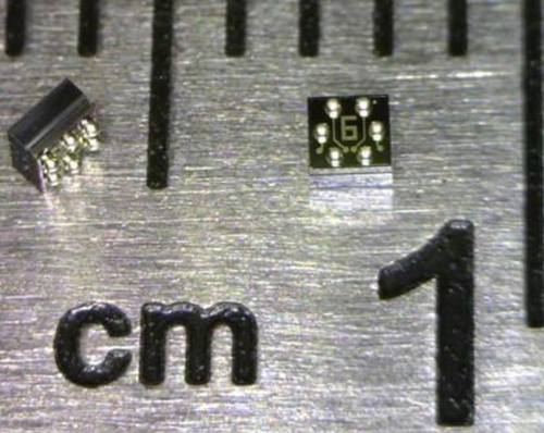
PORTLAND, Ore.—Super-small inertial sensors, like microelectromechanical system (MEMS) three-axis accelerometers, are finding more-and-more uses in ultra-small Internet of Things (IoT) devices such as wearables and industrial and medical devices such as endoscopes that can navigate the smallest tracks, vessels and cavities of our bodies. The mCube Inc. (San Jose, Calif.) 0.9 cubic millimeter three-axis accelerometer—1.1-by-1.1-by-.74 millimeters—was designed specifically for these applications, by making it 75 percent smaller than the 2-by-2 and 3-by-3 millimeter accelerometers sold by its competitors. Samples of mCubes world smallest three-axis accelerometer will be shown for the first time at the MEMS Executive Congress 2015 (Napa, Calif., Nov. 4-to-6).
The three-axis accelerometer from mCube is three years ahead of the competition, according to analysts, at less than one cubic millimeter.
(Source: mCube, used with permission)
The three-axis accelerometer from mCube is three years ahead of the competition, according to analysts, at less than one cubic millimeter.
(Source: mCube, used with permission)
"What we call the Internet of moving things," Ben Lee, chief executive officer (CEO) of mCube told EE Times, "needs the smallest form factor possible, for many applications, and we are the only ones who can supply them today. Analysts tell us we are three years ahead of our competition."
Symmetry is another principle that mCube follows, on the advise of the founding father of MEMS, Kurt Peterson who is famous for saying "symmetry is Godlike." The original mCube three axis accelerometer was 1.6-by-1.6, the current model is 1.1-by-1.1 and its next generation model will be symmetrically sub-millimeter, according to Lee. Peterson emphasizes symmetry because it allows MEMS devices—especially those stacking the MEMS atop the application specific integrated circuit (ASIC) on the same complementary metal oxide semiconductor (CMOS) chip to run without the compensation circuitry required by non-symmetrical architectures, especially those with the MEMS and ASIC on separate chips, according to Lee.
The  mCube vias between the ASIC and the MEMS on a single CMOS chip is 11-to-100 times smaller than the connections used by Invensense and Bosch respectively
(Source: mCube, used with permission)Click here for larger image
The mCube vias between the ASIC and the MEMS on a single CMOS chip is 11-to-100 times smaller than the connections used by Invensense and Bosch respectively
(Source: mCube, used with permission)
Click here for larger image
Throughout each shrinkage only minor changes have been made to mCube's MEMS-on-CMOS architecture which still carries the same 30 micron proof mass--which is 10 micron bigger than its competitors, according to Lee, who claims mCube's large proof mass is what makes its measurements of acceleration more accurate.
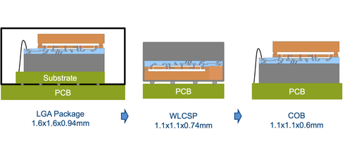
Instead of shrinking the proof mass, mCube has been going to smaller package architecture. For instance, its first 1.6 millimeter square MEMS was in a land-grid array package (LGA), the current 1.1 millimeter square device uses a Wafer Level Chip Scale Package (WLCSP) and its sub-millimeter model due out in the future will go to an even smaller chip-on-board (COB) package so small that it can be housed inside the IoT or medical device's application specific integrated circuit (ASIC) package.
The first mCube three-axis accelerometer was in a land grid array (LGA) package, but the current model downsized it by going to a wafer-scale chip scale package and in the future mCube plans to downsize more to a chip-on-board package that can fit inside other manufacturer's systems-on-chip (SoCs).
(Source: mCube, used with permission) Click here for larger image
The first mCube three-axis accelerometer was in a land grid array (LGA) package, but the current model downsized it by going to a wafer-scale chip scale package and in the future mCube plans to downsize more to a chip-on-board package that can fit inside other manufacturer's systems-on-chip (SoCs).
(Source: mCube, used with permission)
Click here for larger image
The mCube MC3571 accelerometer has the same user configurable 8-,10- or 14-bit output as its predecessor which has shipped over 100 million units, with an output data rate of up to 1,024 bits-per-second over an I2C bus.

http://www.eetimes.com/document.asp?doc_id=1328125

Monday, October 26, 2015

Will Zen save AMD, or might Apple?

There's good news and bad news about struggling chip company AMD (Advanced Micro Devices). The good news is that it has taped out Zen, its next generation microprocessor. The bad news is that its quarterly financial results revealed deepening losses. Revenues fell by 26 percent to $1.06 billion and it made a net loss of $197 million, after writing down $65 million worth of APU inventory. (See: AMD Q3: Revenue beats despite steep decline, but earnings miss.)
But what happens next? Will Zen chips arrive soon enough, and sell well enough, to turn the company's fortunes around? Or could it be rescued by a white knight on a charger, in which case, Apple might be a candidate.
There's no doubt that AMD has fallen behind Intel across the whole PC market. Intel dominates the high end and server markets with its Core iX and Xeon processors, and the low end with Atom-based (but Pentium- and Celeron-branded) processors. AMD may point to superior graphics capabilities, but these have not translated into sales.
The brutal truth is spelled out in AMD's latest financial results. The Computing and Graphics division (desktop and notebook CPUs and GPUs) lost $181 million on sales of only $424 million - down 45 percent year-on-year. The division that provides embedded chips and SoCs (System on a Chip) made a profit of $84 million, which reflects the fact that its SoCs are used in both the Sony PlayStation 4 and Microsoft Xbox One games consoles.
AMD responded by giving its chip designers the freedom to do whatever they wanted to create its seventh-generation CPU design, codenamed Zen. According to Lisa Su, AMD's president and CEO, this will process 40 percent more instructions per clock cycle with Simultaneous Multi-threading (SMT). Desktop processors will have up to eight cores plus a dedicated GPU, with 16- and perhaps 32-core versions coming for servers.
The problem is that the first Zen processor, code-named Summit Ridge, may not appear until October 2016. By that time, Intel should be shipping high-performance versions of Skylake, with Cannon Lake appearing in Ultrabooks and other portables. Just catching Intel won't win AMD many sales: Zen needs to deliver a significant edge, and that's hard to do.
By October 2016, AMD could be in a much worse financial position, and this might make it a tempting take-over target. The question is, who would want it? Qualcomm, Samsung and Mediatek might be possibilities, but what about Apple?
One of the tricky parts of any takeover is that AMD's agreement with Intel could be cancelled. However, Apple could negotiate a new agreement with Intel in advance, and retain the rights to make x86 processors.
With AMD under its wing, Apple could use Zen core designs and AMD's ATI graphics cores to design its own custom SoCs for Macintosh computers, with the manufacturing farmed out to Intel or Global Foundries (ex-AMD) and TSMC.
This would, in essence, repeat what Apple did with ARM processors. It bought an established ARM chip company, PA Semi (Palo Alto Semiconductor), and now designs its own ARM-based SoCs for the iPhone and iPad, with manufacturing farmed out to Samsung and TSMC.
(Incidentally, PA Semi's Jim Keller, who designed Apple's ARM-based SoCs, returned to AMD to lead the Zen development, though he left recently.)
Whether it would be worth it, given the relatively low volume of Mac sales, is another matter. If Apple views the Mac as a very profitable boutique business, it probably isn't. But the option to use cheap custom-designed SoCs to expand the Mac market might be tempting. The possibility of, perhaps, combining Intel x86-compatible and ARM cores on the same SoC might be even more tempting.
Either way, buying AMD would have five obvious advantages for Apple:
1) it would gain the ability to design its own x86-compatible SoCs to replace off-the-shelf Intel chips;
2) it would have access to advanced graphics chip designs such as FirePro (AMD acquired ATI for $5.4 billion in 2006);
3) it would get AMD's advanced ARM chip, code-named K12, which has been co-developed with Zen;
4) it would get AMD's large patent portfolio;
5) it would have more control over its own destiny, which is something Apple values highly.
If AMD keeps piling up losses, it may well be looking for a rescuer in another 12-24 months, and Apple could pay for it without even noticing. The fruit company already has $200 billion in spare cash, and will pile up even more billions in the next two years, so the price is irrelevant.
As far as I know, Apple has no plans to buy AMD, but it's still an interesting thought-experiment. Life would be more boring if Qualcomm bought it.

http://www.zdnet.com/article/will-zen-save-amd-or-might-apple/

Thursday, October 22, 2015

What China Is Planning

With about $120 billion in funding at its disposal, China is looking to buy key technologies it doesn’t already have.
popularity
Over the years, China has unveiled several initiatives to advance its domestic semiconductor industry. China has made some progress at each turn, although every plan has fallen short of expectations. But now, the nation is embarking on several new and bold initiatives that could alter the IC landscape.
China’s new initiatives address at least three key challenges for its IC industry:
1. China continues to lag behind its foreign rivals in IC technology and the nation’s chipmakers hope to close the gap.
2. China consumes nearly 60% of the world’s chips today, but its chipmakers produce less than 10% of the world’s ICs, according to analysts.
3. China must import about 90% of its chips from foreign suppliers, which in turn, has created a staggering $150 billion trade deficit in ICs alone, according to Gartner.
Hoping to solve these problems, China recently launched two major initiatives. Unveiled in June of 2014, the first program is called the “National Guideline for Development of the IC Industry.” In simple terms, the plan is designed to accelerate China’s efforts in several areas, such as 14nm finFETs, advanced packaging, MEMS and memory.
As part of the plan, China created a $19.3 billion fund, which will be used to invest in its domestic IC firms. And over the next decade, local municipalities and private equity firms could spend a whopping $100 billion across China’s IC sector.
Then, in May of 2015, China launched another initiative, dubbed “Made in China 2025.” The goal is to upgrade and increase the domestic content of components in 10 key areas—information technology; robotics; aerospace; shipping; railways; energy systems and vehicles; power equipment; materials; medicine; and agricultural machinery.
In both initiatives, the country hopes to achieve a simple goal. “China wants to be self-sustaining,” said Samuel Wang, an analyst with Gartner. “They want to make everything, including all machinery, instruments and components.”
But if China can’t develop a given technology in a realistic time frame, the government has another plan in place. It will simply acquire a company to obtain the technology.
“China wants to support homegrown semiconductor manufacturers, including the foundries,” Wang said. “Mergers and acquisitions are also part of their strategy. They are looking for missing pieces of the puzzle. What they don’t have they want to acquire. And whatever they already have, they consider the foreign company as being a competitor.”
Indeed, China has embarked on an aggressive acquisition strategy to accelerate its efforts in select markets. In just one of many examples, a group from China recently acquired Singapore’s STATS ChipPAC, a move that put China in the upper echelon in the outsourced assembly and test (Outsourced Semiconductor Assembly and Test) market.
Not all of China’s acquisition plans have panned out, however. For example, China wants a domestic memory maker. So in July, Tsinghua Unigroup, China’s largest chip design company, launched an unsolicited bid to buy Micron Technology for $23 billion. That deal failed to transpire amid national security concerns.
In any case, the questions are clear. Have China and its chipmakers made any progress since launching its various initiatives over 18 months ago? Will China accomplish its goals and what are the challenges?
It’s too complex to look at every industry in China. But to help answer some of these questions, Semiconductor Engineering has taken a look at China’s ongoing efforts to develop three key technologies: 14nm finFETs; memory; and advanced packaging.
Chasing after finFETs
As part of its ambitious plans, China hopes to close the gap in process technology. Semiconductor Manufacturing International Corp. (SMIC), China’s largest foundry vendor, has been tapped by the government to lead the charge.
Today, SMIC is ramping up its 28nm planar technology, but the ultimate goal is to develop 14nm finFET technology by 2020 or sooner.
To help its cause, SMIC, Huawei, IMECand Qualcomm in July formed a joint R&D venture within SMIC’s fab in Shanghai. The venture will develop 14nm finFET technology.
SMIC faces some challenges. FinFETs are difficult to develop. Moreover, it takes technology, know-how, and, of course, money.
So will SMIC succeed? “SMIC should be able to develop 14nm finFETs before the 2020 deadline,” Gartner’s Wang said. “We are still looking at another five years away. By that time, the industry knowledge will be available to develop the technology.”
SMIC will not only get help from Imec, but also the IC equipment industry. “When the equipment guys sell equipment, they more or less provide the recipe to the fab guys to guide them. Today, this is considered confidential information. But after three years they may be able to release such information,” he said.
Even if SMIC is successful, the company will be three to five years behind its competitors. Today, GlobalFoundries, Intel, Samsung and TSMC are ramping up 16nm/14nm finFETs, with 10nm and 7nm in R&D.
Still, SMIC might not be that far behind. Today, the 16nm/14nm finFET rollout is taking longer than expected amid a slew of challenges. Plus, 16nm/14nm finFETs will be a long-running node.
In addition, the 10nm finFET market is also in flux. “If the industry pushes out 10nm, 14nm can be extended,” Wang said. “So, maybe the 14nm market will continue to be there by 2020.”
China has other options. To speed up its efforts in advanced logic, China could make an acquisition. Multiple reports have surfaced that China has talked to GlobalFoundries about an acquisition. A spokesman for GlobalFoundries declined to comment.
“I’m not sure who is making the first move, but now that GlobalFoundries owns the IBM Microelectronics assets, the sale of GlobalFoundries to China would run into major U.S. opposition,” said Joanne Itow, an analyst with Semico Research.
Besides finFETs, China could go down another path. GlobalFoundries, for one, recently held a forum in China to push its 22nm fully depleted silicon-on-insulator (FD-SOI) technology. FD-SOI has some advantages for China’s fabless chipmakers. “It’s easier to design with it,” said Gary Patton, chief technology officer at GlobalFoundries.
China is still evaluating FD-SOI, according to Gartner’s Wang, who added that China is also looking at developing other chip technologies, such as FPGAs, power semiconductors and SSD controllers. “Software programmability is big for FPGAs. So I don’t see that China can easily catch up in FPGAs,” Wang said. “In power management ICs or power MOSFETs, China can catch up.”
Wanted: memories
China imports the vast majority of its memory chips from foreign suppliers, but there is some memory production in that nation. For years, SK Hynix has been producing DRAMs in China.
In 2014, Samsung began ramping up its new 300mm fab in Xi’an, China, which is expected to produce 3D NAND. “(The) Xi’an fab, as we have mentioned, is mainly dedicated to V-NAND,” said Ji Ho Baek, vice president of memory marketing at Samsung, in a recent conference call. “The current ramp-up is being conducted gradually and according to plan. So, in addition to developing new products and enhancing our process capability, we also use the Xi’an fab to respond to the demand for enterprise and high-end datacenter SSDs.”
Then, in October of 2015, Intel announced that its China fab will be converted from the production of 65nm chipsets to 3D NAND and 3D XPoint over the next few years. It expects to begin selling 3D NAND products from this fab in the second half of 2016. Intel plans to invest $5.5 billion in the Dalian-based fab.
In addition, China also boasts one memory foundry vendor. That company, XMC, produces NOR on a foundry basis for Spansion, now part of Cypress. Spansion and XMC are also working on 3D NAND.
It’s also no secret that the Chinese government wants a China-based memory supplier, especially DRAM. Given that it’s too late to start a new memory company, China must acquire the technology.
For example, a Chinese consortium recently entered into a definitive agreement to acquire ISSI, a U.S.-based, niche-oriented memory supplier.
Meanwhile, Tsinghua hasn’t thrown in the towel after making an unsuccessful bid to buy Micron. In fact, Tsinghua and Micron are still in talks about forming a business deal, including a joint fab venture in China, according to multiple sources.
To help with the talks, Tsinghua recently hired Taiwan chip veteran Charles Kau, sources said. Kau recently resigned as chief executive of Nanya, a Taiwan DRAM maker. However, Kau is still chairman of Inotera, a joint DRAM venture in Taiwan between Nanya and Micron.
It won’t be easy to lure Micron to China, though. “Memory manufacturers will look to expand their footprint in China, if they’re able to get preferential incentives and/or funding for fab investments and operations. But this is not at the expense of transferring core technologies or R&D,” said Greg Wong, an analyst with Forward Insights.
Others agreed. “China is trying to get hold of DRAM production for its internal use. But with the preposterous bid for Micron this July and the possible delay in acquiring ISSI, China may have to position itself a bit more friendly to attract more memory makers,” said Alan Niebel, president of Web-Feet Research.
Advances in packaging
For years, China has been a major hub for IC packaging, where OSATs offer competitive pricing. Several OSATs have manufacturing sites in China. In addition, Intel, TI and other multinationals also have IC-packaging manufacturing plants in China.
Meanwhile, China’s domestic OSATs have been smaller players that focused on the Chinese market. Then, in 2014, Jiangsu Changjiang Electronics Technology (JCET), a Chinese OSAT, shook up the landscape by announcing a deal to acquire STATS ChipPAC for $780 million. The deal was completed in August of 2015.
With the acquisition of STATS ChipPAC, JCET jumped from sixth to fourth place in the worldwide OSAT rankings with combined sales of $2.6 billion in 2014, according to Gartner. JCET still trails Taiwan’s ASE ($5.2 billion), U.S.-based Amkor ($4 billion) and Taiwan’s SPIL ($2.7 billion), according to Gartner.
The deal also propels China into the advanced packaging market. Generally, JCET provides low-to-middle pin-count packages. STATS ChipPAC focuses on advanced packaging, such as 2.5D/3D, flip-chip and wafer-level packaging.
JCET is strong in the China market, while STATS’ customers are mainly outside of China. “From a portfolio point of view, there is a good marriage,” said Scott Sikorski, vice president of product technology marketing at STATS ChipPAC, now a subsidiary of JCET. “This also positions us much more strongly to compete with the other tier-one OSATs.”
Analysts agree. “Over the long run, this will probably benefit both STATS and JCET,” said Jan Vardaman, president of TechSearch International, a market research firm.
Still, there are challenges for OSATs in China. “Competing on price alone may not be sufficient (in the China market),” Vardaman said. “In addition, a complex process typically requires trained operators and engineers. A lower operator turnover rate is required. But the turnover rate is very high in China. Retraining an operator every three to four months is detrimental. Yield improvement and more efficient operations are required.”
Meanwhile, the JCET-STATS deal makes sense for other reasons. “The merger will also give us a much bigger access to the China market,” STATS ChipPAC’s Sikorski said.
In fact, the packaging business is heating up in China. For one thing, China’s fabless chipmakers are rapidly migrating towards more advanced designs, which, in turn, require new packaging types.
“As these Chinese brands try to compete on the international stage, they can’t do it with low pin count packaging only,” Sikorski said. “The Chinese customer base requires increasingly more advanced packaging.”


http://semiengineering.com/what-china-is-planning/

Wednesday, October 21, 2015

Intel May Invest as Much as $5.5 Billion in China Chip Plant

Intel Corp., the world’s biggest chipmaker, said it will invest as much as $5.5 billion in its plant in Dalian, China, to convert the factory to production of memory chips.
The plant, which began operations in 2010, will begin manufacturing the devices by the second half of next year, the Santa Clara, California-based company said Tuesday in a statement. Intel said it plans to invest as much as $3.5 billion in the next three to five years, which may subsequently increase to $5.5 billion.
Intel, which gets the majority of its sales from processors, has a joint-venture with Micron Technology Inc. to produce memory chips -- called NAND flash -- that store data in mobile devices and increasingly in computers. By shifting computing from its reliance on magnetic disks to semiconductors for storage, Intel is trying to speed up data access and make laptops, servers and desktops more responsive.
In its most recent quarter, Intel said demand for memory chips helped offset weaker demand for personal-computer processors.
Micron said that it may use supply from the upgraded plant and “could have a greater participation in the future.” No formal decision has been announced, the company said in an e-mailed statement.
Intel shares fell less than one percent to $33.43 at 3:37 p.m. New York time. The stock had declined 7.4 percent this year through Monday’s close. Micron’s stock fell 11 percent to $17.35.

http://www.bloomberg.com/news/articles/2015-10-20/intel-will-invest-as-much-as-5-5-billion-in-china-chip-plant

Tuesday, October 20, 2015

Microsemi Offers to Buy PMC-Sierra in $2.4 Billion Deal

The California chip maker Microsemi Corporation said on Monday that it had offered to acquire its fellow chip maker PMC-Sierra in a cash-and-stock deal valued at about $2.4 billion.
The offer, in the form of a letter to PMC-Sierra’s board of directors on Monday, came as Microsemi sought to derail a competing proposal from Skyworks Solutions, a rival chip maker and supplier to Apple.
Skyworks, based in Woburn, Mass., offered to buy PMC-Sierra for $2 billion in cash this month.
Under the terms of its offer, Microsemi said it would be willing to pay about $11.50 in cash and stock for each share of PMC-Sierra, representing a 50 percent premium to PMC-Sierra’s closing price the day before the Skyworks offer was announced.
Microsemi said that it believed its offer was superior to the Skyworks proposal and provided PMC-Sierra with “substantial premium and immediate cash value.”
“Based on extensive discussions with PMC over the past 18 months and comprehensive analysis, we believe this transaction offers compelling strategic and financial benefits for the shareholders of both Microsemi and PMC,” James J. Peterson, the Microsemi chairman and chief executive, said in a news release.
“This acquisition will provide Microsemi with a leading position in high performance and scalable storage solutions targeted for data center and cloud applications, while also adding a complementary portfolio of high-value communications products,” he added.
The deal would be subject to regulatory and shareholder approval.
PMC-Sierra, based in Sunnyvale, Calif., makes semiconductors for telecommunications networks and data storage. Founded in 1984, it posted revenue of $526 million in 2014 and has about 1,450 employees worldwide.
There has been a wave of consolidation in the semiconductor industry in recent years as chip makers look to increase their scale and product offerings to better serve Apple and other electronics makers, while cutting their costs.
This year alone, Intel, the world’s largest maker of chips; Avago Technologies; and NXP Semiconductors have made multibillion-dollar acquisitions.
In May, Avago agreed to acquire Broadcom, whose chips are used in iPhones and other consumer devices, for $37 billion, while June, Intel agreed to pay $16.7 billion for the chip maker Altera. In March, NXP Semiconductors agreed to buy Freescale Semiconductor for $11.8 billion.
Under the terms of Microsemi’s offer, PMC-Sierra investors would receive $8.75 in cash and 0.0736 of a share of Microsemi stock for each share they hold in PMC-Sierra.
PMC-Sierra shareholders would own about 15 percent of the combined company, with the remainder owned by Microsemi investors, Microsemi said.
Microsemi said its proposal, if accepted, could close as soon as late December if PMC-Sierra’s directors were to act quickly.
Once the deal goes through, Microsemi said, it expects to achieve more than $100 million in annual cost savings.
Microsemi, based in Aliso Viejo, Calif., manufacturers semiconductors for a variety of industries, including the aerospace, communications, defense, security and industrial sectors. It posted sales of $1.14 billion in 2014 and has about 3,600 employees worldwide.
Stifel and the law firm O’Melveny & Myers LLP are advising Microsemi on its offer.

http://www.nytimes.com/2015/10/20/business/dealbook/microsemi-offers-to-buy-pmc-sierra-in-2-4-billion-deal.html?WT.mc_id=SmartBriefs-Newsletter&WT.mc_ev=click&_r=0

Monday, October 19, 2015

Swiss researchers have created a memristor with three stable resistive states - See more at: http://www.newelectronics.co.uk/electronics-news/swiss-researchers-have-created-a-memristor-with-three-stable-resistive-states/108563/#sthash.BPwLUU9d.dpuf

Researchers funded by the Swiss National Science Foundation have created an electronic component that could replace flash storage. This memristor could also be used one day in new types of computers.
The principle of the memristor was first described in 1971, as the fourth basic component of electronic circuits (alongside resistors, capacitors and inductors). Since the 2000s, researchers have suggested that certain types of resistive memory could act as memristors and HP and Intel have entered into a race to produce a commercialised version.
“Memristors require less energy since they work at lower voltages,” explained Jennifer Rupp, professor in the Department of Materials at ETH Zurich. “They can be made much smaller than today’s memory modules, and therefore offer much greater density. This means they can store more megabytes of information per mm2.”
Along with her colleague, chemist Markus Kubicek, Prof Rupp has built a memristor based on a slice of perovskite 5nm thick. She claims that her component has three stable resistive states. As a result, it can not only store the 0 or 1 of a standard bit, but can also be used for information encoded by three states – the 0, 1 and 2 of a ‘trit’.
“Our component could therefore also be useful for a new type of IT that is not based on binary logic, but on a logic that provides for information located ‘between’ the 0 and 1,” continued Prof Rupp. “This has interesting implications for what is referred to as fuzzy logic, which seeks to incorporate a form of uncertainty into the processing of digital information. You could describe it as less rigid computing.”
Another potential application is neuromorphic computing, which aims to use electronic components to reproduce the way in which neurons in the brain process information. “The properties of a memristor at a given point in time depend on what has happened before,” explained Prof Rupp. “This mimics the behaviour of neurons, which only transmit information once a specific activation threshold has been reached.”
Primarily, the researchers at ETH Zurich have characterised the ways in which the component works by conducting electro-chemical studies. “We were able to identify the carriers of electrical charge and understand their relationship with the three stable states,” said Prof Rupp. “This is extremely important knowledge for materials science which will be useful in refining the way the storage operates and in improving its efficiency.”
- See more at: http://www.newelectronics.co.uk/electronics-news/swiss-researchers-have-created-a-memristor-with-three-stable-resistive-states/108563/#sthash.BPwLUU9d.dpuf


Researchers funded by the Swiss National Science Foundation have created an electronic component that could replace flash storage. This memristor could also be used one day in new types of computers.
The principle of the memristor was first described in 1971, as the fourth basic component of electronic circuits (alongside resistors, capacitors and inductors). Since the 2000s, researchers have suggested that certain types of resistive memory could act as memristors and HP and Intel have entered into a race to produce a commercialised version.
“Memristors require less energy since they work at lower voltages,” explained Jennifer Rupp, professor in the Department of Materials at ETH Zurich. “They can be made much smaller than today’s memory modules, and therefore offer much greater density. This means they can store more megabytes of information per mm2.”
Along with her colleague, chemist Markus Kubicek, Prof Rupp has built a memristor based on a slice of perovskite 5nm thick. She claims that her component has three stable resistive states. As a result, it can not only store the 0 or 1 of a standard bit, but can also be used for information encoded by three states – the 0, 1 and 2 of a ‘trit’.
“Our component could therefore also be useful for a new type of IT that is not based on binary logic, but on a logic that provides for information located ‘between’ the 0 and 1,” continued Prof Rupp. “This has interesting implications for what is referred to as fuzzy logic, which seeks to incorporate a form of uncertainty into the processing of digital information. You could describe it as less rigid computing.”
Another potential application is neuromorphic computing, which aims to use electronic components to reproduce the way in which neurons in the brain process information. “The properties of a memristor at a given point in time depend on what has happened before,” explained Prof Rupp. “This mimics the behaviour of neurons, which only transmit information once a specific activation threshold has been reached.”
Primarily, the researchers at ETH Zurich have characterised the ways in which the component works by conducting electro-chemical studies. “We were able to identify the carriers of electrical charge and understand their relationship with the three stable states,” said Prof Rupp. “This is extremely important knowledge for materials science which will be useful in refining the way the storage operates and in improving its efficiency.”


http://www.newelectronics.co.uk/electronics-news/swiss-researchers-have-created-a-memristor-with-three-stable-resistive-states/108563/

Friday, October 16, 2015

Prelude to 5G: Qualcomm, Huawei Muscle into V2X

MADISON, Wis.—Huawei and Qualcomm, two cellular technology giants, are muscling their way into the nascent vehicle-to-vehicle (V2V), vehicle-to-infrastructure communication market, often collectively titled V2X, by proposing a new LTE standard called “LTE V2X.”
The move is at odds with incumbent automotive technology suppliers who have been working more than a decade to develop and test — and finally implement — a Dedicated Short-Range Communications (DSRC) technology designed for V2V, V2I communications.
DSRC, based on the IEEE 802.11p standard, uses a dedicated wireless frequency — 75 MHz of spectrum in the 5.9GHz band — allocated by the Federal Communications Commission in 1999 specifically for intelligent transportation systems.
Meanwhile, proponents of LTE V2X are pitching LTE-based cellular network infrastructure as the basis of V2X. They claim that LTE Direct (LTE-D), also known as LTE Device-to-Device (D2D), offers a good foundation for LTE V2X development. LTE-D is said to enable discovery of thousands of devices and their services within 500 meters, thus allowing two or more proximal LTE-D devices to communicate within the network.
The result of these developments is a connected-car clash between the DSRC faction, and others jockeying for a foothold in the automotive industry in the anticipation of the emerging 5G cellular network standard. Cellular players are counting on 5G to offer native support for automotive-related communications.
As EE Times talked to several automotive technology vendors last week during Intelligent Transportation System (ITS) World Congress in Bordeaux, many were visibly unhappy about last-minute efforts by Huawei and Qualcomm to push an alternative V2X communication technology.
Lars Reger, chief technology officer of NXP’s Automotive business unit, believes DSRC has already come a long way. The technology, which has cleared a number of field tests over the years, is about to go inside new connected cars. Noting that LTE V2X is still in development, Reger estimated substantial delays before the new standard is finished, tested and accepted by the automotive industry.
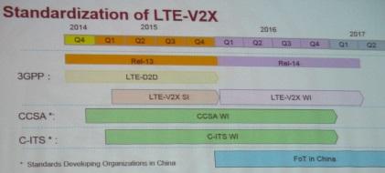
Huawei's timeline shows the LTE-V2X Study Item completing its work by the end of this year. The LTE-V2X Work Item begins in 2016.
(Source: Huawei)
Huawei’s timeline shows the LTE-V2X Study Item completing its work by the end of this year. The LTE-V2X Work Item begins in 2016.
(Source: Huawei)
Driven by whom?
So, here’s the question. Do carmakers now see something wrong with designing DSRC into their cars, after mulling it over and dragging their heels for more than 15 years?
When EE Times asked Huawei if carmakers have asked them to develop an alternative V2X technology, Jiansong Gan, technical director, connected car at Huawei, paused a second and said, “That’s a good question.”
But he pointed out that the advantage of promoting LTE-based V2X is that a “LTE cellular network infrastructure already exists.”  There is no need to build a V2X infrastructure afresh to support DSRC.
Gan also cited the potential interference issues of 5.8GHz DSRC in China and explained, “In China, we need a different V2X solution.”  The Chinese Communication Standards Association (CCSA) already launched a Work Item for LTE-based V2X in China.
Asked about the emerging conflict between DSRC and LTE V2X, Guang Yang, senior analyst responsible for wireless operator strategies at Strategy Analytics, called DSRC “still the mainstream technology for V2X.” He added, “Technically speaking, DSRC has nothing wrong, I think.”
Yang explained that the main target of LTE for V2X isn’t necessarily to solve any problem [with DSRC], “but to create new business opportunity for cellular industry.”
DSRC vs. LTE V2X
Let’s break down the DSRC vs LTE V2X issue.
As Huawei’s Gan argued, the biggest advantage of LTE V2X is that it could reuse the existing cellular infrastructure and spectrum. Strategy Analytics’ Yang said, “Operator needs not to deploy dedicated road side unit (RSU) and apply dedicated spectrum.”
Meanwhile, DSRC is using IEEE 802.11p, essentially a half-clocked 802.11a system. It is an approved amendment to the IEEE 802.11 standard that adds wireless access in vehicular environments and communication systems.  Calling DSRC essentially “a Wi-Fi based technology,” Yang said, “So in theory, LTE could provide better quality of service than DSRC.”
On the flip side, though, Yang said, “LTE-based V2X technology is more complex and the market size is smaller than Wi-Fi. Currently DSRC’s standard is ready now, but LTE V2X is still in study phase.” He added, “LTE could bring some enhancements but may generate new problems.”
Not everyone believes that LTE is a better way to go for V2X, especially when a crisis hits.

Nir Sasson, CEO of Autotalks, told EE Times, “I was in Japan on March 11, 2011, when the great earthquake and tsunami hit the nation. It took me more than 20 minutes to send a text message to my wife.”
Recalling how cellular services in Japan ground to a halt, Sasson said, “I don’t think we want to depend on the cellular network infrastructure for V2X.”
Autotalks has been working with STMicroelectronics to deliver V2X chipset families – one as a V2X complete, standalone solution and another as V2X hardware add-on solution. Autotalks said it will deliver a mass market-optimized V2X chipset for widespread deployment by 2017.
According to the LTE-V2X presentation by Huawei made at a July ITU Workshop in Beijing, LTE-V2X proponents pointed out several issues with 802.11p-based DSRC deployment.
They claim, for example, that performance “cannot be guaranteed, since 802.11p is an ad-hoc mechanism.” They also note that spectrum dedicated for V2V road safety is limited to 10MHz for the United States, and 30MHz for Europe. Aside from the cost of deploying roadside telematics units, they say the business model for DSRC isn’t clear and, perhaps more important, there is “no clear evolution path for future services.”
In contrast to DSRC, Huawei stresses that LTE-V2X, aside from reusing mobile network operator’s network infrastructure, is “one [LTE] chipset for all, allowing lower integration costs for car OEMs.”
The road to standardization
LTE-V2X still faces a long road to standardization, not to mention commercial deployment. Huawei’s timeline shows the LTE-V2X Study Item completing its work by the end of this year. The LTE-V2X Work Item begins in 2016.
The study at 3GPP (3rd Generation Partnership Project) is co-led by Huawei, LGE and CATT, a local telecom equipment manufacturer in China.
Noting that LTE V2X is still in its study phase in 3GPP, Strategy Analytics’ Yang told EE Times that after the study, it will become a Work Item in 3GPP Release 14 for formal standardization.
“According to the 3GPP schedule, the Release 14 standard should be completed in 2017. After the standard is done, it usually takes at least one year to produce a commercial chipset.”
Realistically speaking, “LTE V2X could not be available for commercial application until 2018 or even later,” he concluded.
Warm up to 5G
Leading the charge for LTE V2X are Qualcomm and Huawei. Smaller players such as LGE and CATT are also pushing it, observed Yang. He noted that big mobile network operators such as Deutsche Telecom and Orange (France) “are also happy to see the progress.”
Because LTE V2X is based on LTE-D2D, “Qualcomm is the major IPR owner,” said Yang. Other players, including Chinese companies, are “trying to enhance LTE-D2D in order to meet V2X requirements, in addition to decrease Qualcomm’s IPR share.”
Given the time needed for LTE V2X development, during which the cellular industry is presumably also busy discussing 5G, wouldn’t LTE V2X become a short-lived interim standard?
Yang noted, “It could be warm-up for 5G. Through the LTE V2X discussion, the cellular industry could prepare the necessary technical solutions (some of them could be reused in 5G), and build consensus within the industry as well as with the external partners.”
The level of support the development of LTE for V2X from carmakers remains unclear. Yang simply put, “I think it is just pushed by cellular industry.”
He explained, “Some automotive manufacturers have been involved in 5G research. For example, BMW is a partner of EU research project METIS (short for ‘Mobile and wireless communications Enablers for 2020 Information Society’) — which is a flagship research project for 5G. But I haven’t seen that they are eager for LTE V2X.”

http://www.eetimes.com/document.asp?_mc=RSS_EET_EDT&doc_id=1328030&page_number=1

Wednesday, October 14, 2015

Intel Falls on Projected Slowdown in Corporate Server Demand

Intel Corp. declined after saying a slowdown in demand from corporations threatens to curb sales at its server-chip division -- one of the few bright spots at a company beset by a personal-computer slump.
The world’s largest chipmaker reported third-quarter results that reflected the anemic PC market and forecast fourth-quarter revenue that was in line with analysts’ estimates. Sales in the current period will be $14.8 billion, plus or minus $500 million, Intel said Tuesday in a statement. On average, analysts projected $14.8 billion, according to data compiled by Bloomberg.
On a conference call, Intel executives reduced their target for growth in the server group, a division the company has relied on for sales and profit growth in recent years as the PC market contracts. Corporations, especially in China, are scaling back on server purchases as they outsource more of their technology needs and delay updating their in-house equipment. Chief Executive Officer Brian Krzanich said he remains confident that over time the unit will return to growth of about 15 percent, from a percentage in the low-double digits this year.
“There has been some slowing in enterprise spending,” Alex Gauna, an analyst at JMP Securities in San Francisco, said before the report. He has the equivalent of a hold rating on the stock. “There has to be slowing out there. There are too many macro headwinds.”
Intel shares, down 13 percent this year, slipped 2 percent to $31.38 at 10:53 a.m. Wednesday in New York.
Separately on Wednesday, the European Commission cleared Intel Corp.’s $16.7 billion acquisition of Altera Corp., saying the combination will continue to face effective competition in Europe.

Third Quarter

Third-quarter net income fell to $3.11 billion, or 64 cents a share, from $3.32 billion, or 66 cents, in the same period last year. Revenue was little changed at $14.5 billion. On average, analysts had projected earnings of 59 cents on sales of $14.2 billion.
Gross margin, or the percentage of sales remaining after deducting cost of production, was 63 percent in the third quarter. That measure, the only indicator of profit that Intel predicts, will be about 62 percent this quarter.
Third-quarter sales in the company’s client-computing group, which includes PC and mobile chips, fell 7.5 percent from a year earlier to $8.51 billion. Data-center unit revenue jumped 12 percent to $4.14 billion. Intel’s so-called Internet of Things group, which supplies semiconductors for all sorts of connected devices, posted a 9.6 percent gain in sales to $581 million, while software and services was little changed.

PCs vs. Servers

Intel’s processors power more than 80 percent of PCs sold, making its results a harbinger of demand across the computer industry. The Santa Clara, California-based chipmaker’s report leads off several weeks of earnings announcements by the largest technology companies.
While Intel got more than twice as much revenue from selling PC chips as it did from its data-center group in the recent period, the two units brought in almost the same amount of operating profit. That change has been driven by Intel’s 99 percent market share in server chips and surging demand for the machines from operators of data centers, such as Amazon.com Inc. and Google, which are building up their capacity to provide computing power, storage and services via the Internet.
“What we saw were good growth rates in data center, memory and the Internet of Things business that was offsetting some of the weakness that we’ve been seeing in the PC segment,” said Intel Chief Financial Officer Stacy Smith. “We would expect to see a normal uptick in consumer buying in the fourth quarter in the PC segment and we’ll continue to see growth in the other segments.”
Global PC shipments fell 7.7 percent in the third quarter, hurt by slower desktop sales and higher dollar-based prices, Gartner Inc. said last week. PC manufacturers shipped 73.7 million units, compared with 79.8 million a year earlier, the market researcher said.

http://www.bloomberg.com/news/articles/2015-10-13/intel-s-sales-forecast-points-to-strong-data-center-chip-demand

Tuesday, October 13, 2015

Infineon CEO Says Robot Cars Will Drive Semiconductor Demand

Infineon’s CEO, Reinhard Ploss, says that the autonomously driven cars of the future will create a large demand for a variety of new semiconductors and sensors. Speaking in a keynote address at SEMI’s Semicon Europa’s Fab Manager’s Forum in Dresden, Germany, Ploss outlined the “drivers” behind the evolution of robot cars and autonomous cars and what we might expect in terms of semiconductor requirements.
Ploss expects a slow evolution to fully autonomous cars, but eventually the experience may be no different than what stepping into an elevator and pushing a button is like today.
Among the many advantages of autonomous driving:
  • Traffic fatalities (1.3 million deaths a year across the globe) can be reduced, as 90% of all accidents are caused by human errors
  • Less traffic congestion: Today, US commuter spend 38 hours/year in traffic jams, which are causing total costs of $121 billion/year
  • Increasing commuter productivity, as time in car can be used for e.g. working (48 min/day per average American)
  • Improved fuel efficiency (up to 50%)
  • Offering mobility for everybody, e.g. disabled, elder or young people
  • Reduction of accidents enables lower insurance rates
Figure 1 shows how automotive safety has evolved over time, and where increased automation is likely to come into play. Ploss said in the five levels of autonomous driving – assisted, partially automated, highly automated and fully automated – everything is still under the control of the driver in the fourth, highly automated, stage.
Figure 1
“Traffic management is a huge opportunity when you have a connected autonomously driving car,” Ploss said. “If you manage traffic to go smoothly at a lower speed, or even the same speed as the trucks, then you have the optimum load for the road.”
“As we move on the, the next big step for automated driving will be on highways,” Ploss said it will take some time to get to fully automated driving. “You need rules on how you can operate. Think about a small Italian village where you have a road which is good for one car. Who goes first?”
An automated car must have the ability for:
  • Recognizing surrounding: roads, traffic participants, traffic signs
  • Speed and direction control: motor, brakes, steering
  • Monitoring of driver
It enables:
  • Assisted/Automated driving
  • Free time while commuting Higher road efficiency (platooning) Automated parking
  • Emergency assist, e.g. braking
Ploss also touched on the advantages and challenges in connecting cars to the internet. “Many believe the autonomous driving car must be a connected car. If we connect to the internet, we can gain more information, and even add capabilities to the car,” he said.
The connected car requires ability for:
  • V2X connections
  • Infotainment, real-time maps, adverts
  • Fleet/network management
It enables:
  • V2X aids automated driving, e.g. road condition, weather info
  • More safety by further ‘looking ahead’
  • Vehicle on demand and ride sharing
  • Traffic flow management
  • Remote servicing, e-Call
Ploss said an automated car will require an “unbelievable” number of sensors. “It will look like a cocoon going around,” Ploss said. Figure 2 shows the number of cameras, radar and Lidar (laser-based radar) we’ll likely see if future generations of cars.
Figure 2
“The car will become a unit with a lot of sensors in order to recognize what is going on. These signals have to be computed, so you also have a very high level of computing power in the car to process this data,” he said.
In addition, the various motors and actuators will be required to apply brakes and steer the car. “When you see something going on the road, you have to take the right action in order to brake, steer away, etc. You have to be able to do it under a certain reliability,” Ploss said.
As in airplanes, there will be some redundancy built in, although Ploss said he believe 2X redundancy will be sufficient (vs 3X in airplanes). “Two times redundancy will be something we see more and more,” he said.
In terms of added semiconductor content, Ploss said a partially automated car will have about $100 in added in semiconductor content (today’s cars already have about $330 in semiconductor content. A highly automated car would have $400 added and a fully automated would have about $550 (Figure 3).
Figure 3
“When you look at the engine, there is a huge need for microcontrollers, sensors and power semiconductors,” Ploss said. “When you go for the hybridization, the pure electrical vehicle, it’s all about semiconductors because the efficiency of the electric drive train is highly dependent on how you are running the engine and how you regain the power when you are braking.”
Ploss added that reducing CO2 emissions was another important aspect of automotive electronic demand. “In today’s combustion engine, there is still a lot of potential to reduce the CO2 emissions. You need an awful lot of sensors and controls in order to run this engine at a very high efficiency. A significant improvement can still be done (for gas and diesel),” he said.
One challenge for the semiconductor industry is to innovate while reducing costs. “We have to go in two directions – innovation for new and better functionality and innovation for cost reduction,” Ploss said. He noted that cost reductions from the pure shrink is “not coming so easy” but sees potential in the Industry 4.0 movement. “When you have a fully connected manufacturing then you can get a lot of data that enables you to learn faster and to manufacture at zero defects,” he said.
Another challenge is that radar employs high frequency GHz electronics (Figure 4). “High frequency brings a lot of specialization,” Ploss said. He said mixed-signal bipolar will first be used, but “as we move to 20nm and 14nm, we will be able to have CMOS-based processes.”
Figure 4
He noted the advantages of silicon carbide for switching applications, citing a 50% loss reduction compared to a silicon solution. This could improve the efficiency of electric vehicles by 3% he noted. “When you think about electric driving, you always think about the last percentage point of gaining efficiency. SiC has a huge potential to enable this. It is a wide bandgap material and you can much smaller size, higher switching frequency, less conduction losses at the higher switching frequency,” he said.
Already, car manufacturers have shown autonomous concept cars, such as the Mercedes Benz F 015.

Tags: , , , ,

http://semimd.com/blog/2015/10/12/infineon-ceo-says-robot-cars-will-drive-semiconductor-demand/

Wednesday, October 7, 2015

Massachusetts Man Sentenced to 37 Months in Prison for Trafficking Counterfeit Military Goods

A Massachusetts man was sentenced today to 37 months in prison for importing thousands of counterfeit integrated circuits (ICs) from China and Hong Kong and reselling them to U.S. customers, including contractors supplying them to the U.S. Navy for use in nuclear submarines.
Assistant Attorney General Leslie R. Caldwell of the Justice Department’s Criminal Division, U.S. Attorney Deirdre M. Daly of the District of Connecticut, Special Agent in Charge Matthew J. Etre of U.S. Immigration and Customs Enforcement’s Homeland Security Investigations (ICE-HSI) in New England, Special Agent in Charge Craig W. Rupert of the Defense Criminal Investigative Service (DCIS) Northeast Field Office and Special Agent in Charge Leo Lamont of the Naval Criminal Investigative Service (NCIS) Northeast Field Office made the announcement.
Peter Picone, 42, of Methuen, Massachusetts, pleaded guilty on June 3, 2014, to conspiracy to traffic in counterfeit military goods.  In addition to imposing the prison term, U.S. District Judge Alvin W. Thompson of the District of Connecticut ordered Picone to pay $352,076 in restitution to the 31 companies whose ICs he counterfeited, and to forfeit $70,050 and 35,870 counterfeit ICs.
“Picone risked undermining our national security so that he could turn a profit,” said Assistant Attorney General Caldwell.  “He sold counterfeit integrated circuits knowing that the parts were intended for use in nuclear submarines by the U.S. Navy, and that malfunction or failure of the parts could have catastrophic consequences.”
“Supplying counterfeit electronic components to the U.S. Military is a serious crime,” said U.S. Attorney Daly.  “Individuals who choose profit over the health and safety of the men and women of our armed services will be prosecuted.”
“Counterfeit electrical components intended for use in U.S. military equipment put our service members in harm’s way, and our national security at great risk,” said Special Agent in Charge Etre.  “HSI will continue to aggressively target individuals and companies engaged in this type of criminal act.”
“The sentencing today demonstrates the continued efforts of the Defense Criminal Investigative Service and our fellow law enforcement partners to protect the integrity of the Department of Defense's infrastructure,” said Special Agent in Charge Rupert.  “Distributors who opt for financial gain by introducing counterfeit circuitry into the supply chain of mission critical equipment create an environment ripe for potential failures.  Such disregard puts the warfighter at an unnecessary risk, ultimately impacting the mission readiness of our military that the nation depends on.  DCIS will continue to shield America's investment in Defense by addressing all attempts to disrupt the reliability of our military's equipment and processes.”
“The U.S. Navy submarine force is a critical component of our national security,” said Special Agent in Charge Lamont.  “Protecting the Sailors who make up that force and their supply lines are top priorities for NCIS, to ensure our strategic deterrent remains effective.”
In April 2015, Picone founded Tytronix Inc., and served as its president and director until August 2010, when the company was dissolved.  In addition, from August 2009 through December 2012, Picone owned and operated Epic International Electronics (Epic) and served as its president and director.
In connection with his guilty plea, Picone admitted that, from February 2007 through April 2012, first through Titronix and later through Epic, he purchased millions of dollars’ worth of ICs bearing the counterfeit marks of approximately 35 major electronics manufacturers, including Motorola, Xilinx and National Semiconductor, from suppliers in China and Hong Kong.  Picone admitted that he resold the counterfeit ICs to customers both in the United States and abroad, including to defense contractors that Picone knew intended to supply the counterfeit ICs to the U.S. Navy for use in nuclear submarines, among other things.  Picone further admitted that he knew that malfunction or failure of the ICs likely would cause impairment of combat operations and other significant harm to national security.
On April 24, 2012, federal agents searched Picone’s business and residence, and recovered 12,960 counterfeit ICs.  In connection with his guilty plea, Picone admitted that he intended to sell the seized counterfeit ICs to defense contractors doing business with the Navy for use in military applications.
The case was investigated by the Defense Criminal Investigative Service, the NCIS and ICE-HSI.  The case is being prosecuted by Senior Counsel Kendra Ervin and Evan Williams of the Criminal Division’s Computer Crime and Intellectual Property Section (CCIPS), Assistant U.S. Attorney Sarala Nagala and Special Assistant U.S. Attorney Carol Sipperly of the District of Connecticut, Trial Attorney Anna Kaminska of the Criminal Division’s Fraud Section and Trial Attorney Kristen Warden of the Criminal Division’s Asset Forfeiture and Money Laundering Section.  The CCIPS Cybercrime Lab provided significant assistance.
The enforcement action announced today is related to the many efforts being undertaken by the Department of Justice Task Force on Intellectual Property (IP Task Force).  The IP Task Force supports prosecution priorities, promotes innovation through heightened civil enforcement, enhances coordination among federal, state, and local law enforcement partners, and focuses on international enforcement efforts, including reinforcing relationships with key foreign partners and U.S. industry leaders.  To learn more about the IP Task Force, go to www.justice.gov/dag/iptaskforce.

http://www.justice.gov/opa/pr/massachusetts-man-sentenced-37-months-prison-trafficking-counterfeit-military-goods-0