Friday, April 29, 2016
Cypress Semi to buy Broadcom's Internet of Things business
Chipmaker Cypress Semiconductor Corp said it agreed to buy Broadcom Ltd's Internet of Things (IoT) business and related assets for $550 million in cash.
The deal is expected to close in the third calendar quarter and will help Cypress gain share in consumer IoT market, which includes wearable electronics and home automation.
Separately, Cypress said Chief Executive Thurman Rodgers would step down this week.
(Reporting by Supantha Mukherjee in Bengaluru; Editing by Maju Samuel)
http://www.reuters.com/article/us-broadcom-assets-cypress-semicond-idUSKCN0XP1V0
Thursday, April 28, 2016
AMD’s Polaris will be a mainstream GPU, not high-end
AMD's upcoming Polaris 10 and Polaris 11 graphics chips won't be
powering high-end graphics cards, according to recent comments by AMD.
In its latest financial report, the company noted that Polaris 11 would
target "the notebook market," while Polaris 10 would target "the
mainstream desktop and high-end gaming notebook segment."
In an interview with Ars, AMD's Roy Taylor also confirmed that Polaris would target mainstream users, particularly those interested in creating a VR-ready system.
"The reason Polaris is a big deal, is because I believe we will be able to grow that TAM [total addressable market] significantly," said Taylor. "I don't think Nvidia is going to do anything to increase the TAM, because according to everything we've seen around Pascal, it's a high-end part. I don't know what the price is gonna be, but let's say it's as low as £500/$600 and as high as £800/$1000. That price range is not going to expand the TAM for VR. We're going on the record right now to say Polaris will expand the TAM. Full stop."
While those after a successor to the likes of high-end graphics cards like the Fury and Fury X may be disappointed, that Polaris is a mainstream part doesn't necessarily mean it's underpowered. The minimum specs for a VR system call for an Nvidia GTX 970 or an AMD Radeon 290 (or its near-identical replacement the 390), both of which currently retail for around £250.
"If you look at the total install base of a Radeon 290, or a GTX 970, or above, it's 7.5 million units. But the issue is that if a publisher wants to sell a £40/$50 game, that's not a big enough market to justify that yet. We've got to prime the pumps, which means somebody has got to start writing cheques to big games publishers. Or we've got to increase the install TAM."
AMD's recent statements are seemingly contrary to those made by its graphics head, Raja Koduri, in January of this year. In an interview with VentureBeat, Koduri explained that one of the Polaris GPUs was a larger, high-performance GPU designed to take back the premium graphics card market currently dominated by rival Nvidia. It now appears that he was simply referring to bringing high-performance down to a more reasonable price point.
"When we set out to design this GPU, we set a completely different goal than for the usual way the PC road maps go," explained Koduri at the time. "Those are driven by 'the benchmark score this year is X. Next year we need to target 20 percent better at this cost and this power.' We decided to do something exciting with this GPU. Let's spike it so we can accomplish something we hadn't accomplished before."
Full details on AMD's Polaris graphics cards are expected at Computex at the end of May, while Nvidia is expected to reveal details on its Pascal graphics architecture around the same time. Both of the upcoming products have been through the rumour mill multiple times, with some suggesting that Polaris will continue to use HBM1—thus limiting the cards to 4GB of memory—while others suggest that they'll simply use plain old GDDR5.
Meanwhile, Nvidia unveiled its first Pascal graphics card, the monstrous Tesla P100, which is designed for data centres. While the P100 features HBM2 memory—with a crazy-wide 4096-bit bus—rumours suggest the consumer cards will use GDDR5X, an improved version of GDDR5 intended to compete with HBM. There have even been a few shots of the PCB and shroud for the Pascal cards, but take those with a very large grain of salt.
http://arstechnica.co.uk/gadgets/2016/04/amd-polaris-will-be-a-mainstream-gpu/
Wednesday, April 27, 2016
IBM lines up all-flash storage to help power cognitive computing
IBM is expanding its flash storage lineup to power cloud data centers that carry out so-called cognitive computing.
The company’s newest FlashSystem arrays, introduced Wednesday, combine its fast and relatively affordable FlashCore technology with a scale-out architecture designed to be easy to expand.
Cognitive computing, which IBM defines as real-time data analysis for immediate, automated decision-making, is at the heart of much of IBM’s current technology push for enterprises and service providers. Its Watson technology is the star of the show but only the most visible part of what the company is doing in this space. An example of cognitive computing is a mobile operator analyzing information about phone call quality to make decisions on the fly about changes in the network, said Andy Walls, an IBM Fellow and CTO for flash systems.
Large-scale, real-time computing needs flash, IDC analyst Eric Burgener said.
“You basically can’t run that stuff on hard disk drives, because the latencies are way too slow,” Burgener said. IBM, like other vendors, wants to make flash work for the fast-growing Web-scale world.
To build scale-out flash arrays suited to these kinds of applications, IBM combined its FlashCore hardware with its Spectrum Accelerate software for easy expansion and streamlined management. FlashCore is flash media IBM builds right onto boards as an alternative to pre-built SSDs (solid-state drives). Other vendors like EMC and Violin Memory are using similar boards, which are designed to be faster and more economical than SSDs.
On Wednesday, IBM introduced an all-flash appliance, the FlashSystem A9000, and a rack-based version of the same system, called the A9000R. They’re the first products in IBM’s all-flash lineup designed for cognitive computing, Walls said.
IBM is also adding data deduplication and compression that it says won’t delay data delivery.
Another feature, Hyper-Scale Mobility, can move data among arrays without disrupting operations. FlashSystem arrays do this by learning an organization’s usage patterns over time.
The A9000 is an appliance designed for hyperscale and cloud storage in mid-sized enterprises. It can retune itself when customers add more storage, and its mangement software lets administrators run more than 100 appliances from one user interface.
The A9000R is a petabyte-scale rack-based system for large enterprises and cloud service providers. It’s designed for multiple tenants and has quality-of-service features to make sure one tenant doesn’t monopolize network or processing capacity at the expense of others. IBM will custom-build these systems for customers, saving them configuration work.
The A9000 and A9000R systems will be available this week, priced as low as US$1.50 per gigabyte, IBM said.
Also on Wednesday, the company introduced the DS8888, an all-flash storage array optimized for IBM’s z Systems and Power Systems mainframe platforms.
http://www.cio.com/article/3061879/ibm-lines-up-all-flash-storage-to-help-power-cognitive-computing.html
Tuesday, April 26, 2016
SK Hynix Sees Improvement After Profit Drops to 3-Year Low
SK Hynix Inc., an Apple Inc. supplier, predicted memory-chip shipments
will start to improve after a dismal first quarter, when the company
reported its lowest operating profit in three years on sluggish demand
for smartphones and computers.
The chipmaker’s shares climbed 6 percent to 29,150 won at the close on Tuesday, the biggest jump since August 2015, after the company said it anticipates DRAM shipment growth of about 15 percent in the second quarter.
That could be a sign that demand for memory-chip prices will start to pick up, after sputtering growth in China and other markets hurt sales of electronics products from smartphones to personal computers. Prices for DDR3 4-gigabit dynamic random access chips averaged $1.81 in the latest period, compared with $3.42 a year earlier, according to data from inSpectrum Inc. DRAM chips, along with NAND flash memory, are used in smartphones, tablets, personal computers and game consoles.
"Based on the company’s outlook, investors are now thinking the company earnings will look prettier in the second quarter than what they had previously thought," Claire Kim, an analyst at Daishin Securities Co., said. "The company’s shipment growth forecast seems aggressive and that is setting a positive tone on the overall semiconductor industry, including its chief rival Samsung Electronics."
Still, Hynix’s operating income slumped 65 percent to 561.8 billion won ($489 million) in the three months ended March, the lowest since the first quarter of 2013, the Icheon, South Korea-based company said in a filing Tuesday. That compares with the 593.4 billion-won average of analyst estimates compiled by Bloomberg.
Hynix posted consolidated net income excluding minority interest of 444.2 billion won, compared with 1.3 trillion won a year earlier.
"We are anticipating more positive demand momentum around the second half," Joonho Kim, president and head of corporate support at SK Hynix, said during a conference call following the first-quarter results.
http://www.bloomberg.com/news/articles/2016-04-25/sk-hynix-posts-lowest-profit-in-three-years-as-chip-prices-tank
Friday, April 22, 2016
Next-Generation Chips Hit a Snag
As chipmaking advances have run up against the limits of physics,
threatening to push up manufacturing costs, the industry’s leaders have
placed a great deal of faith in a Dutch company called ASML. For most of
the past decade, ASML has been promising that its new technique
for creating transistors would allow chips to keep getting slimmer and
more powerful at the rates we’re used to. In 2012, Intel, Samsung, and
TSMC took the unprecedented step of investing about $1.6 billion in ASML
to speed its research and paid close to $5 billion for 23 percent of
the company.
ASML expects to ship as many as seven new machines this year so chipmakers can start testing the technology, known as extreme ultraviolet lithography (EUV). Chief Executive Officer Peter Wennink says most of his customers expect to incorporate EUV by 2019, and he’s prepping for orders within the next year. “The industry needs EUV,” he says.
So far, though, the technology for EUV is proving less efficient than once thought and possibly unable to deliver the returns investors hoped for. Even alternatives that would make smartphone and PC parts costlier have started to look more attractive, says Patrick Ho, an analyst at investment bank Stifel Nicolaus. “The industry made their bet several years ago that EUV would be the next generation,” he says. “It’s been very disappointing.” TSMC declined to comment for this story. Samsung didn’t respond to a request for comment.
Lithography is the process of using concentrated rays of light to burn lines into layers of materials deposited on silicon, a crucial step in creating transistors—and a natural choke point for engineers working at a near-atomic level. These days, companies are trying to etch lines smaller than the wavelength of the light used to do the work, hence the push into extreme ultraviolet beams with shorter wavelengths. “Without EUV … your economics are worse,” says Weston Twigg, an analyst at Pacific Crest Securities. “If EUV is not ready, things get a lot harder.”
The problem is that beams with shorter wavelengths use a lot of energy, and ASML’s machines require substantial downtime because EUV dirties the mirrors used in the process. According to its public statements, ASML aims to cut the EUV machine’s required downtime, from the current 25 percent to 30 percent, to 20 percent by yearend. Not exactly what you want to hear when the price tag (even without the research and development funding) runs to eight figures, making it the most expensive device in the plant.
Stifel Nicolaus’s Ho says ASML, one of Europe’s few technology powerhouses, has to prove it can keep to its schedule. Its latest, that is. In 2007, former CEO Eric Meurice said EUV machines would be cost-effective for chipmakers by 2012. Says Pacific Crest’s Twigg: “It’s probably the most advanced scientific research program in the world. Yet the program is still behind.”
In February, TSMC co-CEO Mark Liu told investors that his company has backup plans. That month, Intel’s director of lithography strategic sourcing, Janice Golda, wrote in a company blog post that the question with EUV is when, not if. But, she added, “the road to EUV lithography production is a long one.” Chipmakers tend to incorporate manufacturing advances in two- to three-year cycles, so if EUV isn’t ready this year, ASML’s next big chance would be closer to 2020.
For now, the most obvious way to get smaller lines is to use current lithography techniques a greater number of times on each chip. The big chipmakers have been loath to do that because it takes longer, always top of mind in a $10 billion factory that will be obsolete within five years. Yet the complex nature of EUV development should be the bigger concern, says Robert Maire, president of Semiconductor Advisors. “There are so many things that can go wrong,” he says. “We may never see a payback on the investment and time put into EUV.”
http://www.bloomberg.com/news/articles/2016-04-21/next-generation-euv-chips-hit-a-snag
Thursday, April 21, 2016
Qualcomm Falls on Concern Apple May Switch to Another Chipmake
Apple Inc. may be going in a new direction for a crucial iPhone
component that connects the handset to the Internet, and such a
suggestion caused Qualcomm shares to tumble.
Qualcomm Inc., the world’s largest maker of chips that go inside smartphones, indicated on an earnings call Wednesday that it may be losing some orders from Apple for modem chips that link the iPhone to the web. Qualcomm Chief Executive Officer Steve Mollenkopf told analysts he is “assuming” that a major customer will give orders to a rival, indicating a potential loss of business for the company.
Analysts said they think the customer is Apple. Apple and Samsung Electronics Co., are the San Diego-based chipmakers’ biggest customers, according to data compiled by Bloomberg. Samsung already uses multiple suppliers, leaving only Apple to make this change.
Any switch Apple makes to suppliers that provide the components inside its devices can send ripples across the industry. Qualcomm’s stock fell in extended trading after Mollenkopf made his comments. Analysts including Tim Arcuri at Cowen & Co. have speculated that Apple may be partnering with Intel Corp. for the modem chip inside the iPhone.
Qualcomm stock fell 2.5 percent, to $50.80, at 10:00 a.m. in New York Thursday. The shares were up 4.2 percent this year through Wednesday.
Mollenkopf made the comments in the context of assuring analysts that the company can deliver profit at the levels it has predicted even if its largest customers give some orders to other suppliers.
“We think there is an element of investor expectation that they lose some business at Apple,” said Sid Parakh, a fund manager for Becker Capital Management, which owns Qualcomm stock.
A Qualcomm spokesman said the company isn’t commenting beyond what was said on the conference call. Apple declined to comment.
While other mobile phone makers use a combination of processor and modem, usually from Qualcomm, Apple designs its own processors and uses separate modems, which are chips that connect the phone to cellular networks.
http://www.bloomberg.com/news/articles/2016-04-20/apple-s-potential-switch-for-key-iphone-component-hits-qualcomm
Qualcomm Inc., the world’s largest maker of chips that go inside smartphones, indicated on an earnings call Wednesday that it may be losing some orders from Apple for modem chips that link the iPhone to the web. Qualcomm Chief Executive Officer Steve Mollenkopf told analysts he is “assuming” that a major customer will give orders to a rival, indicating a potential loss of business for the company.
Analysts said they think the customer is Apple. Apple and Samsung Electronics Co., are the San Diego-based chipmakers’ biggest customers, according to data compiled by Bloomberg. Samsung already uses multiple suppliers, leaving only Apple to make this change.
Any switch Apple makes to suppliers that provide the components inside its devices can send ripples across the industry. Qualcomm’s stock fell in extended trading after Mollenkopf made his comments. Analysts including Tim Arcuri at Cowen & Co. have speculated that Apple may be partnering with Intel Corp. for the modem chip inside the iPhone.
Qualcomm stock fell 2.5 percent, to $50.80, at 10:00 a.m. in New York Thursday. The shares were up 4.2 percent this year through Wednesday.
Mollenkopf made the comments in the context of assuring analysts that the company can deliver profit at the levels it has predicted even if its largest customers give some orders to other suppliers.
Investor Expectation.
Investors didn’t appear to be reassured.“We think there is an element of investor expectation that they lose some business at Apple,” said Sid Parakh, a fund manager for Becker Capital Management, which owns Qualcomm stock.
A Qualcomm spokesman said the company isn’t commenting beyond what was said on the conference call. Apple declined to comment.
While other mobile phone makers use a combination of processor and modem, usually from Qualcomm, Apple designs its own processors and uses separate modems, which are chips that connect the phone to cellular networks.
http://www.bloomberg.com/news/articles/2016-04-20/apple-s-potential-switch-for-key-iphone-component-hits-qualcomm
Wednesday, April 20, 2016
ASE, SPIL say supply not affected by Japan quake
IC packagers Advanced Semiconductor Engineering (ASE) and
Siliconware Precision Industries (SPIL) have said their supply chains
will not be affected by two major earthquakes that struck Kumamoto
Prefecture in Japan on April 14 and 16.
ASE indicated
operations at its manufacturing site in Takahata, Yamagata, which was
acquired from NEC in 2004, were not affected by the recent powerful
earthquakes.
ASE's production base in Yamagata offers
BGA packaging and other backend services for analog, digital and
mixed-signal ICs. Monthly sales generated from the site are estimated at
around US$100 million.
SPIL noted one of its suppliers
which provides QFN substrate materials halted production due to the
quakes. But with SPIL's dual-source strategy, there is no impact on
SPIL's operations, the company said.
ASE's share price
closed at NT$35.25 (NT$1.09) on the Taiwan Stock Exchange (TSE) on April
19, up NT$0.95, while SPIL's fell NT$0.65 to close at NT$49.85.
http://www.digitimes.com/news/a20160419PD206.html
Monday, April 18, 2016
Chipmakers betting big on solid state drive storage system
Competition in the global solid-state drive market is heating up as more
players are rolling out the storage system built on technology that
stacks cells vertically.
An SSD is lighter and more compact than a conventional hard disk drive. It also boasts shorter booting time and faster reading and writing speeds than an HDD.
Intel recently rolled out a new SSD lineup based on 3-D NAND flash memory in Seoul, home turf of Samsung Electronics, the largest SSD manufacturer by sales in the world.
David Lundell, director of Intel’s client SSD strategic planning and product marketing division, said at a press meeting last week that the U.S. chip powerhouse would up the ante in the SSD business in a bid to catch up with Samsung.
“Intel invested 6 trillion won ($5.2 billion) in Dalian, China in October last year to turn a semiconductor factory into one that produces storage systems (SSDs),” said the marketing director, adding that the U.S. chip company would run full throttle to take the lead in the burgeoning SSD market.
The 3-D NAND flash memory chips incorporated in Intel’s newly released SSDs have 32 layers of cells, considered the second generation of its kind.
Samsung, which introduced the world’s first SSD with 3-D chip stacking technology in 2013, is producing third-generation SSDs boasting 48 layers of cells.
Enjoying first-mover advantage, Seoul-based Samsung currently remains an unparalleled market leader with a 38 percent market share by sales, outrunning No. 2 Intel by 24 percentage points in 2015, according to market research firm IHS.
Samsung earned $5.4 billion last year, up from $4 billion the year before, while Intel’s revenue for its SSD business stood at $1.9 billion.
SanDisk, Micron and Toshiba follow the two, capturing 10 percent, 6 percent and 5 percent of market share, respectively.
SK hynix, the world’s second-largest DRAM maker by sales, has also ratcheted up its efforts to increase its footing in the SSD segment. It released its first 3-D NAND SSD products in Shenzhen, China last week, which according to the firm can read a 2-gigabyte, or two-hour long, movie file in one second. The SK Group affiliate took 11th place with 2 percent market share last year.
IHS forecast that the world’s SSD market will grow from $14.1 billion in 2015 to $18.8 billion in 2020.
http://www.koreaherald.com/view.php?ud=20160417000244
An SSD is lighter and more compact than a conventional hard disk drive. It also boasts shorter booting time and faster reading and writing speeds than an HDD.
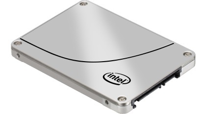 |
| Intel’s solid-state drive product (Intel) |
Intel recently rolled out a new SSD lineup based on 3-D NAND flash memory in Seoul, home turf of Samsung Electronics, the largest SSD manufacturer by sales in the world.
David Lundell, director of Intel’s client SSD strategic planning and product marketing division, said at a press meeting last week that the U.S. chip powerhouse would up the ante in the SSD business in a bid to catch up with Samsung.
“Intel invested 6 trillion won ($5.2 billion) in Dalian, China in October last year to turn a semiconductor factory into one that produces storage systems (SSDs),” said the marketing director, adding that the U.S. chip company would run full throttle to take the lead in the burgeoning SSD market.
The 3-D NAND flash memory chips incorporated in Intel’s newly released SSDs have 32 layers of cells, considered the second generation of its kind.
Samsung, which introduced the world’s first SSD with 3-D chip stacking technology in 2013, is producing third-generation SSDs boasting 48 layers of cells.
Enjoying first-mover advantage, Seoul-based Samsung currently remains an unparalleled market leader with a 38 percent market share by sales, outrunning No. 2 Intel by 24 percentage points in 2015, according to market research firm IHS.
Samsung earned $5.4 billion last year, up from $4 billion the year before, while Intel’s revenue for its SSD business stood at $1.9 billion.
SanDisk, Micron and Toshiba follow the two, capturing 10 percent, 6 percent and 5 percent of market share, respectively.
SK hynix, the world’s second-largest DRAM maker by sales, has also ratcheted up its efforts to increase its footing in the SSD segment. It released its first 3-D NAND SSD products in Shenzhen, China last week, which according to the firm can read a 2-gigabyte, or two-hour long, movie file in one second. The SK Group affiliate took 11th place with 2 percent market share last year.
IHS forecast that the world’s SSD market will grow from $14.1 billion in 2015 to $18.8 billion in 2020.
http://www.koreaherald.com/view.php?ud=20160417000244
Friday, April 15, 2016
It’s All About DRAM
For decades, the starting point for compute architectures was the
processor. In the future, it likely will be the DRAM architecture.
Dynamic random access memory always has played a big role in computing. Since IBM’s Robert Dennard invented DRAM back in 1966, it has become the gold standard for off-chip memory. It’s fast, cheap, reliable, and at least until about 20nm, it has scaled quite nicely.
There is plenty of debate about what comes next on the actual DRAM roadmap, whether that is sub-20nm DRAM or 3D DRAM. DRAM makers are under constant pressure to shrink features and increase density, but there are limits. That helps explain why there is no DDR5 on the horizon, and why LPDDR5 is the last in line for mobile devices.
All of this ties directly into compute architectures, where the next shift may be less about the process used to create the memory than where the memory is placed, how it is packaged, and whether a smaller form factor is useful.
There are several options on the table in this area. The first, the Hybrid Memory Cube (HMC), packs up to eight DRAM chips on top of a logic layer, all connected with through-silicon vias and microbumps. This is an efficient packaging approach, and it has been proven to be significantly faster than the dual in-line memory modules (DIMMs) found in most computers and mobile devices. But it’s also proprietary and may never achieve the kinds of economies of scale that DRAM is known for.
HMC was introduced in 2011, but systems using these chips didn’t start rolling out commercially until last year. The problem for HMC is that the second generation of high-bandwidth memory, a rival approach, also began rolling out last year. HBM likewise packs up to eight DRAM chips and connects them to the processor using a silicon interposer. HBM has a couple of important advantages, though. First, it is a JEDEC standard. And second, there are currently two commercial sources for these chips—SK Hynix and Samsung.
A third approach, which Rambus is exploring, is to put DRAM on a single card that can be shared by racks of servers in a data center. The goal, as with the other memory approaches, is to limit the distance that huge amounts of data have to travel before back and forth to be processed. This approach shows some merit in the cloud world, where huge data centers need a solution for minimizing distances that data needs to travel.
The key in all of these approaches is understanding that it isn’t the processor that is the bottleneck in compute performance anymore. It’s the movement of data from one or more processor cores in and out of memory. Processor cores, regardless of whether they are CPUs, GPUs, MPUs or even DSPs, generally run fast enough for most applications if there is an open path to memory. Just turning up the clock speed on processors doesn’t necessarily improve performance, and the energy costs are significant. Those costs can be measured in data center operating costs and and mobile device battery life.
The two big knobs for boosting performance are more efficient software (a subject for another story), and faster movement of data in and out of memory. While multiple levels of embedded SRAM help improve processor performance for some basic functionality, the real heavy lifting on the memory side will continue to involve DRAM for the foreseeable future. That requires a change in memory packaging and I/O, but in the future it also will become a driver for new packaging approaches for entire systems, from the SoC all the way up to the end system format.
New memory types will come along to fill in the spaces between SRAM and DRAM—notably MRAM, ReRAM and 3D XPoint—but there will always be a need for a more efficient DRAM configuration. What will change is that entire chip architectures will begin to wrap around memories rather than processors, softening the impact of what arguably is one of the biggest shifts in the history of computing.
http://semiengineering.com/its-all-about-dram/
Thursday, April 14, 2016
Intel Begins Shipping Xeon Chips With FPGA Accelerators
Combining the Intel server chips with Altera's FPGAs will improve the performance-per-watt of systems running the two by 70 percent, officials say.
Intel has begun shipping a development module that features the company's latest Xeon E5 server processors and programmable chips that will help customers drive performance while holding down power consumption. The multichip platform is pairing the 14-nanometer Xeon E5-2600 v4 "Broadwell" processors—launched late in March—with the Stratix 10 field-programmable gate arrays (FPGAs) from Altera. Diane Bryant, senior vice president and general manager of Intel's Data Center Group, on April 13 announced during a keynote address at the company's Intel Developer Forum (IDF) in China that the modules were shipping. Intel and other chip makers are increasingly relying on accelerators to help improve the performance and energy efficiency of their processors and speed up the workloads that run on them. Nvidia and Advanced Micro Devices offer GPU accelerators. However, the company also is now using FPGAs, which can be reprogrammed through software after they've been manufactured. They're becoming more important for cloud and Web-scale environments, where workloads can change quickly. Intel for several years had partnered with Altera to take advantage of the company's technology. Intel now has brought the company in-house, earlier this year completing the acquisition of Altera, which the chip maker bought for $16.7 billion. Intel officials have said the goal is to eventually integrate the FPGAs onto the same die as the CPU.ntel is not only relying on FPGAs for CPU acceleration. The company also has a growing portfolio of Xeon Phi chips, which are x86-based co-processors that can act either as accelerators or as primary chips. In addition, Intel is partnering with eASIC to bring application specific integrated circuits (ASICs) to custom Xeons to be used in enterprise data centers and cloud environments for such workloads as data analytics and security. The goal is to offer customers a broad range of choices.
http://www.eweek.com/servers/intel-begins-shipping-xeon-chips-with-fpga-accelerators.html
Tuesday, April 12, 2016
Cadence buys chip design co Rocketick for $40m
The Israeli startup helps chip makers reduce time to market of new designs by up to 30%.
US company Cadence Design Systems Inc. (Nasdaq: CDNS) has acquired Israeli startup Rocketick Technologies Ltd. Cadence said that Rocketick's technology speeds up its chip development capabilities several times over.
No financial details about the deal were disclosed but sources close to the deal say that Cadence could be paying up to $40 million.
Founded in 2008 by CEO Rocketick Inc. Uri Tal, CEO & VP R&D Rocketick Technologies Ltd. Tomer Ben-David and CTO Shay Mizrachi, who all served in the IDF 8200 Intelligence Unit, and based in Ramat Gan, Rocketick helps chip manufacturers reduce the overall time to market of new chip designs by up to 30%. Its flagship product, RocketSim, solves functional verification bottlenecks by complementing simulators with a multicore processor based co-simulator acceleration solution, offering over 10X faster simulations for highly complex designs. Investors in the company include Intel Capital and Nvidia.
Ben-David said, "Rocketick and Cadence serve market-leading customers whose exploding verification challenges are testing the limits of conventional simulators. Rocketick's technology has been proven to deliver as much as 30X faster simulation on very challenging designs at top tier system and semiconductor companies. We are very excited to join the Cadence team and look forward to providing even more benefit to customers through the tight integration of Rocketick's core engines with Cadence's overall verification solution."
Cadence SVP and general manager of the System & Verification Group and the Digital & Signoff Group Dr. Anirudh Devgan said, "Ensuring that SoC verification is completed on time within ever shrinking project schedules is driving the strong need to speed up the underlying logic simulation technology. Rocketick is the leading, established provider of parallel simulation technology. I look forward to welcoming the Rocketick team to Cadence as we accelerate our innovation in functional verification to solve our customers' most difficult challenges."
Rocketick's 25 employees in Israel will join Cadence's Israel R&D operations. Cadence has offices in Petah Tikva, Rosh Ha'ayin and Haifa. In 2005, Cadence acquired Israeli electronics design solutions company Verisity for $280 million.
Peregrine Ventures general partner and Incentive Incubator CEO Lior Shahory who accompanied Rocketick from the day it was established, said, "When we invested in Rocketick, most of Israel's venture capital funds did not want to take the risk involved in investing in the chip sector. Moreover, Rocketick aspired to provide a complex product with huge technological challenge. One of the factors, which led us to this investment, was the quality of the entrepreneurs, three modest but impressive chip professionals. Another factor which contributed to the investment was the support from Israel's Technological Incubators Program, which provides additional evidence to the key contribution of this program to the growth and development of Israel's technology industry."
http://www.globes.co.il/en/article-cadence-buys-chip-design-co-rocketick-for-40m-1001116678
Monday, April 11, 2016
NXP Said to Weigh Sale of $2 Billion Standard Chips Business
NXP Semiconductors NV, which last year merged with Freescale
Semiconductor Ltd., is weighing a sale of its standard products
business, people familiar with the matter said.
NXP may seek at least $2 billion for the unit, which makes diodes, transistors and other standard chip products, according to the people. The business has drawn interest from Chinese suitors including Jianguang Asset Management Co., the Beijing-based investment firm known as JAC Capital, the people said, asking not to be identified as the process isn’t public.
Bidders from China, seeking to develop a local semiconductor supply chain, have faced setbacks in their pursuit of technology assets after the U.S. government expressed concerns over national security. In January, Royal Philips NV scrapped the $2.8 billion sale of its lighting-components business to a Chinese consortium following opposition from the Committee on Foreign Investment in the United States, or CFIUS.
NXP’s standard products unit, which accounted for one-fifth of its sales last year, mass produces chips used in phones, television sets and cars. A spokesman for NXP, based in the southern Dutch city of Eindhoven, declined to comment. A representative for JAC Capital declined to comment.
“It makes total sense, and it has been discussed before,” Anand Srinivasan, an analyst for Bloomberg Intelligence, said by phone. “It fits in with the company’s strategy and management’s desires.”
Shares of NXP rose 2.8 percent to $83.60 at 10:01 a.m. in New York, after jumping the most in a month, valuing the company at about $29 billion.
State-owned JAC Capital acquired NXP’s radio frequency chip unit for about $1.8 billion last year in a deal that helped smooth regulatory approval for the Freescale merger. In February last year, NXP said it plans to form a Chinese joint venture with JAC Capital.
NXP, which is now the biggest chip supplier to the automotive industry, has shifted to supplying chips for secure processing and connectivity since completing the Freescale merger. Revenue from the standard products unit fell 3 percent to $1.24 billion last year, while it booked operating profit of $264 million.
http://www.bloomberg.com/news/articles/2016-04-08/nxp-said-to-consider-sale-of-2-billion-standard-chips-business
Friday, April 8, 2016
Nvidia is interacting with hundreds of deep-learning startups
Nvidia chief executive Jen-Hsun Huang said that deep-learning
artificial intelligence has become a new computing platform, and the
company is dealing with hundreds of startups in the space that plan to
take advantage of the platform.
Speaking at the GPUTech conference in San Jose, California, Huang noted that $5 billion was invested last year in A.I. startups, and there are probably a thousand companies working on the technology for applications ranging from face recognition to self-driving cars.
“Deep learning is not an industry,” he said. “Deep learning is going to be in every industry. Deep learning is going to be in every application.”
The computational complexity of Go is nearly infinite. But Google’s Alpha Go A.I. was able to beat the best human Go player. It runs on 200 graphics processing units (GPUs).
“It’s a pretty amazing achievement,” he said. “Every single year, we do more and more in this area. We think this will change computing. Deep learning is that significant. It’s a new platform. After working on this for five years, it is our fastest-growing business.”
Deep learning has one general algorithm with many different versions. The team at Baidu was able to deconstruct both English and Chinese with the same algorithm. Now the algorithm can be used with massive amounts of data and huge amounts of processing power to yield big benefits in things like computer vision.
“It started in research and moved to computer platform providers,” he said. “They are incorporating it into frameworks and engines. These are the tools of modern network design, the authoring tools for neural networks.”
Nvidia’s CUDA programming language allows these software frameworks and cloud platforms to tap the power of GPU chips.
“Industry after industry is taking advantage of deep learning,” Huang said. “It’s like Thor’s Hammer that fell from the sky. It’s relatively easy to apply.”
http://venturebeat.com/2016/04/05/nvidia-is-interacting-with-hundreds-of-deep-learning-startups/
Thursday, April 7, 2016
Microchip completes Atmel deal, cuts price
Microchip
has completed its acquisition of Atmel, but has reduced the purchase
price by an undisclosed amount in light of what it calls ‘disappointing
performance’ since it struck the deal.
According to Microchip, Atmel’s net sales for the quarter ended 31 March 31 2016 are expected to be around $220million – more than 15% lower than at the mid point of the previous quarter.
Microchip also noted that it is treating Atmel’s mobile touch business as an asset held for sale. However, touch technology sold to automotive and industrial customers will be retained.
“While the starting point of the size of Atmel’s business is smaller than we originally modelled, it does not fundamentally change the value proposition to Microchip. We understand Atmel’s business well and plan to rapidly integrate Atmel into Microchip,” Sanghi added.
Meanwhile, Microchip expects net sales for its fiscal fourth quarter to be more than $552m.
- See more at: http://www.newelectronics.co.uk/electronics-news/microchip-completes-atmel-deal-cuts-price/117496/#sthash.OSpwB88N.dpuf
Microchip has completed its acquisition of Atmel, but has
reduced the purchase price by an undisclosed amount in light of what it calls
‘disappointing performance’ since it struck the deal.
Steve Sanghi,
pictured, Microchip’s chairman and CEO, said: “The performance of Atmel since
we engaged in discussions in August 2015 has been disappointing. We believe the
large drop in Atmel revenue in the March 2016 quarter is likely the result of
an inventory correction in the distribution channel as distributors reduced
inventory levels, overall weak business conditions, and concerns on the part of
distributors surrounding the impact of the sale of Atmel to Microchip. We took
some of this weakness into consideration in dropping the final acquisition
price from our original offer.”
According to Microchip, Atmel’s net sales for the quarter ended 31 March 31
2016 are expected to be around $220million – more than 15% lower than at the
mid point of the previous quarter. Microchip also noted that it is treating Atmel’s mobile touch business as an asset held for sale. However, touch technology sold to automotive and industrial customers will be retained.
“While the starting point of the size of Atmel’s business is smaller than we originally modelled, it does not fundamentally change the value proposition to Microchip. We understand Atmel’s business well and plan to rapidly integrate Atmel into Microchip,” Sanghi added.
Meanwhile, Microchip expects net sales for its fiscal fourth quarter to be more than $552m.
http://www.newelectronics.co.uk/electronics-news/microchip-completes-atmel-deal-cuts-price/117496/
Wednesday, April 6, 2016
Samsung's First 10-Nanometer DRAM Is 30 Percent Faster
Your RAM’s about to get an upgrade. Samsung has announced
the world’s first 10-nanometer 8-gigabit DRAM chips, and it promises
that they’ll be 30 percent faster and 20 percent more efficient than
what went before.
The new memory chips use a much smaller 10-nanometer manufacturing
technique than the 20-nanometer version that Samsung’s been using since
2014. That allows it to create circuitry in its memory chips with
features that measure just 10-nanometers in size, allowing it to squeeze
more onto the same piece of silicon. And that means improvements in speed and efficiency. Samsung claims its new chips will transfer data at up to 3,200 megabits per second (30 percent faster than the 2,400Mbps that its old 20-nanometer chips managed) while also using 10 to 20 percent less power.
http://gizmodo.com/samsungs-first-10-nanometer-dram-is-30-percent-faster-1769323626
Tuesday, April 5, 2016
Samsung extends its lead in DRAM sector
Samsung Electronics, the world’s second largest semiconductor firm, has
achieved a breakthrough in the global chip sector by successfully
mass-producing a 10-nanometer-class DRAM chip, the company said Tuesday.
The new 8-gigabit double-data-rate-4 (DDR4) DRAM chip -- based on 1x nanometer chip design and manufacturing technology -- will place the Seoul-headquartered chipmaker in an unrivaled position, according to the firm.
Three letters x, y, and z are used to describe the scale of the chip technology with the three representing high-, mid-, and low-single digits, respectively.
Samsung’s 10nm-class chip technology boasts a 30-percent higher production capacity than a 20nm-class chip technology.
A nanometer is one billionth of a meter and a human hair is around 75,000 nanometers in diameter.
Market analysts said Samsung deployed an 18nm chip design and manufacturing technology for DRAM.
“The 18nm DRAM chip will give Samsung an upper hand in price competiveness as its rivals, including SK hynix of Korea and Micron of the U.S., are still focused on 25nm DRAM chips,” said Doh Hyun-woo, an analyst from Mirae Asset.
“Samsung will continue to widen its lead over the runner-ups in the world’s DRAM sector,” he added.
Pressed to fast catch up with Samsung, SK hynix chief executive Park Sung-wook announced earlier this year that the company would complete the development of its own 18nm DRAM chip in the latter half this year and begin the mass-production of the DRAM chip early next year.
Micron saw its sales drop 30 percent on-year to $2.93 during the December-February period with its operating loss coming in at $5 million, down from $855 million a year before.
Samsung’s latest 18nm chip technology has been deployed in PCs and laptops and will be later utilized for mobile and data server products.
“In the near future, we will also launch next-generation, 10nm-class mobile DRAM products with high densities to help mobile manufacturers develop even more innovative products that add to the convenience of mobile device users.” Jun Young-hyun, president of Samsung’ memory business.
The 10nm-class DRAM for mobile devices will be rolled out later this year, according to the tech giant.
http://www.koreaherald.com/view.php?ud=20160405000694
Monday, April 4, 2016
FinFET's Father Forecasts Future
SANTA CLARA, Calif.—Don’t worry about the end
of Moore’s law, there are plenty of good ideas on the semiconductor road
map, according to Chenming Hu, a university researcher credited as
being the father of the FinFET.
Hu described new transistor concepts that could fuel the chip industry for decades in a talk at the annual Synopsys Users Group event here.
His presentation came a day after the company’s chief executive
expressed similar optimism, citing progress in software design tools.“I really mean it when I say this industry goes on another 100 years, in part because there are no alternatives and the world needs us,” Hu told an audience of several hundred chip designers here.
“We all know but don’t like to say out loud that transistor size reduction is a game that has an end and we are racing to that end,” but that doesn’t mean the end of the semiconductor industry and the high tech sector build on top of it, Hu said.
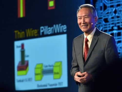
Chenming Hu sees a long future for thin-body transistors like FinFETs and FD-SOI. (Images: Synopsys)
“Essentially it puts a voltage amplifier into the dielectric…the idea is you get the same performance at lower Vdd,” Hu explained.
The design could help engineers reduce Vdd to levels below 0.3 V, overcoming limits that could pave the way to decades of new devices.
The NC-FET has “not been on anyone’s radar because we’ve been developing it on a shoestring but now we see it’s promising and we’re looking for support,” said Hu. “There are orders of magnitude more money going into spintronics than NC-FET, I think we are the only ones in the industry working on it,” he said.
Recently, Berkeley set up a new center to focus on the NC-FET. Intel and TSMC joined, paying $140,000 each. “If we could get a handful of members we could do great things, and that’s still smaller than a typical government contract,” he said.
Separately a handful of companies including Globalfoundries, Samsung, Synopsys and TSMC joined the Berkeley Device Modeling Center that creates BSIM models that translate physical fab data for software design tools.
“We are preparing the compact models for new devices wherever they come from free of royalty, but nothing is really free,” Hu said noting the models for FinFETs took 11 years work from more than a dozen researchers.
http://www.eetimes.com/document.asp?doc_id=1329333
Friday, April 1, 2016
Intel Announces New Chips for Cloud Computing
Intel Corp. announced new chips targeting cloud computing as well as
partnerships to address concerns of companies that have stayed on the
sidelines of that technology trend.
Read full article: http://www.wsj.com/articles/intel-announces-new-chips-for-cloud-computing-1459463097
Read full article: http://www.wsj.com/articles/intel-announces-new-chips-for-cloud-computing-1459463097
Subscribe to:
Comments (Atom)