Wednesday, April 1, 2015

3D Qualcomm SoCs by 2016

PORTLAND, Ore. — The future of three-dimensional (3D) very large scale integration (VLSI) for system-on-chips (SoCs) will not stack die connected by through-silicon-vias (TSVs), but will build them on a single layered die, according to Karim Arabi, vice president of engineering at Qualcomm speaking at the International Symposium on Physical Design (ISPD-2015, Mar. 29-April 1).
"Our 3D VLSI technology, which we call 3DV, enables die size to be shrunk in half, while simultaneously increasing yields," Arabi told us.
Qualcomm's motivation, according to Arabi, is market share in the 18 billion smartphones that he predicts will be produced by 2018 — "more than all the computers and other electronic devices combined," he told us. He also noted that even though the cloud is offloading some computationally intensive applications — such as speech recognition — there will still be an increasing need for local processing power for most smartphone functions.
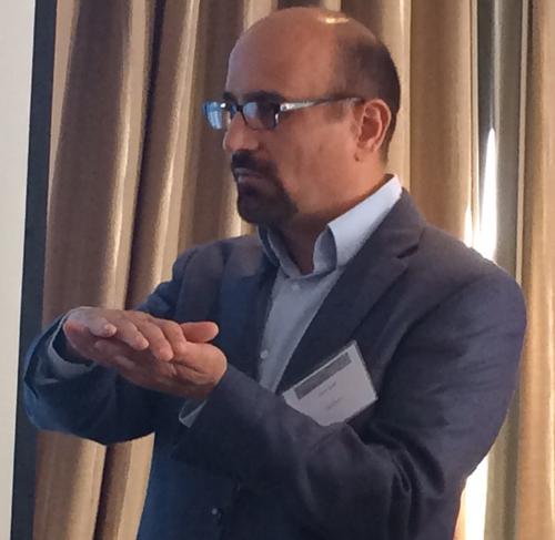
Karim Arabi, vice president of engineering at Qualcomm describes how its next-generation SoCs will use up to three layers without through-silicon-vias (TSVs) to reduce die size and increase yields.
(Source: EETimes)
Karim Arabi, vice president of engineering at Qualcomm describes how its next-generation SoCs will use up to three layers without through-silicon-vias (TSVs) to reduce die size and increase yields.
(Source: EETimes)
In the long term, Qualcomm is building neural processing units (NPUs) modeled on the human brain, "because they are highly flexible and highly efficient for the next generation of mobile devices, cloud computing, Big Data processing, deep learning and machine learning," Arabi told us. But for the near term, Qualcomm is extending the capabilities of its already popular SoCs with its new type of 3DV interconnection and process technology.
Qualcomm is creating two basic types of 3DV interconnection methods with the hope of deploying them by 2016. These new types of 3D interconnection comes in two flavors face-to-back (F2B) and face-to-face (F2F).
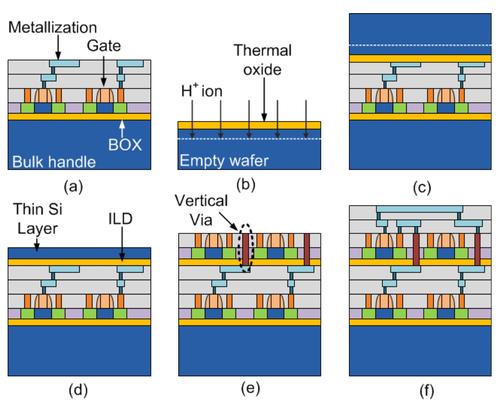
In the fabrication process of front-to-back (F2B) 3DVs (a) the bottom tier is created the same way as 2D-ICs. (b,c,d) To add another layer, first a thin layer of silicon is deposited on top of the bottom tier. (e) This front-end-of-line (FEOL) process of the top tier permits the addition of normal vertical vias and top-tier contacts.  (f) Finally back-end-of-line (BEOL) processing creates the top-tier. 
(Source:Qualcomm)
In the fabrication process of front-to-back (F2B) 3DVs (a) the bottom tier is created the same way as 2D-ICs. (b,c,d) To add another layer, first a thin layer of silicon is deposited on top of the bottom tier. (e) This front-end-of-line (FEOL) process of the top tier permits the addition of normal vertical vias and top-tier contacts. (f) Finally back-end-of-line (BEOL) processing creates the top-tier.
(Source:Qualcomm)
F2B is easier because it doesn't need precision bonding but instead just puts a thin layer of silicon on top of the finished first layer and starts building the second layer using traditional vias. Unfortunately, the bottom layer was likely produced using temperatures as high as 1,200 degrees Celsius. The next layer, however, will have to limit temperatures in order to keep from liquidating layer one's copper interconnects, which have a melting point of 1,085 degrees Celsius. To solve, Qualcomm could use tungsten as interconnects on layers one, which are slightly slower, but have a melting point of 5,930 degrees Celsius. A second solution would be to limit the temperatures on the top level, to say 625 degrees Celsius, which would lessen the performance of the second layer transistors by 27.8 percent for PMOS and 16.2 percent for NMOS. Thus the ideal 3D chip is unachievable today using F2B, overall sacrificing about 37 percent in performance and 41 percent in power.
F2F, on the other hand, allows both chips to use copper interconnects and optimally performing transistors, but has the disadvantage, according to Arabi, that the F2F method requires larger vias the size of which are limited by the accuracy with which the two facing wafers can be bonded. Qualcomm, however, believes that by using a mix of the two techniques it will be able to produce fully optimized 3DV SoCs with an unlimited number of layers. In fact, with appropriate partitioning and floor planning, Arabi believes 3DV chips can be produced that are faster, smaller, consume less power and operate at lower temperatures than putting the same functions on a single 2-D chip.
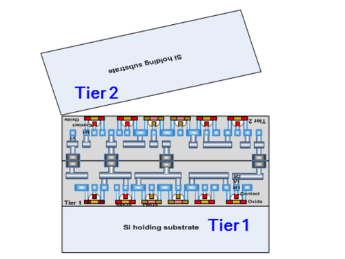
In the fabrication process of front-to-front (FF) 3DVs requires wafer-level bonding and hence the vias can only be a small as the accuracy of the bonding method.
(Source: Qualcomm)
In the fabrication process of front-to-front (FF) 3DVs requires wafer-level bonding and hence the vias can only be a small as the accuracy of the bonding method.
(Source: Qualcomm)
The final advantage of 3DV chips, according to Arabi, is that you only need to use the most expensive and latest node technology on the bottom layer. For instance, the bottom layer housing the CPU, GPU and other high-speed devices can be fabricated at 10-to-14 nanometer, whereas the higher layers housing less critical functions can be fabricated at a less expensive relaxed node of, say, 28-nanometers. He also predicted that the best yielding SoCs will only use two layers, whereas three layers will likely only be used for customers who also want to integrate radio frequency (RF) functions on the top layer.

http://www.eetimes.com/document.asp?doc_id=1326174

No comments:

Post a Comment