Monday, August 31, 2015

Intel Investment Spotlights Drones’ Opportunity for Chipmakers

SAN FRANCISCO—Intel Corp. said Thursday (Aug. 27) it has invested more than $60 million in Chinese drone maker Yuneec Holding Ltd., the clearest indication yet of the opportunity that Intel and fellow chip makers see in the nascent commercial drone space.
“We’ve got drones on our roadmap that are going to truly change the world and revolutionize the drone industry,” said Brian Krzanich, Intel’s CEO, in a video announcing the deal.
In a very short period of time, drones have gone from being viewed as pricey hobbyist toys to an enticing technology with serious commercial applications, including agriculture, construction, product delivery and others.
According to a report published in January by ABI Research Inc., the small unmanned aerial vehicle market will be worth more than $8.4 billion by 2018. The report predicts that commercial drone revenue will grow at a compound annual growth rate of 51% from 2014 through 2019. By 2019, the commercial drone market will be worth roughly five times as much as the hobbyist drone market and more than twice as much as the market for military and civil service drones, according to the report.
[Listen: Pros and Cons of Drones Why regulate?]
Chipmakers, including both Intel and Qualcomm, have taken notice, investing in companies that supply drones and drone technology. According to Dan Kara, practice director for robotics at ABI Research, chip vendors and consumer electronics firms are looking at the drone market as another market where technologies that have been developed mainly for smartphones, such as processing and high-quality imaging technologies, can be applied.
“It’s just opening up another avenue for them [chip vendors] to sell product to,” Kara said.
Krzanich said Intel believes the Yuneec deal will be “a game changer in the drone industry.” He added that Intel believes “drones have the potential to positively change lives in many ways, whether that’s delivering consumer goods or inspecting disaster sites.”
Intel said it would collaborate with Hong Kong-based Yuneec on future products. A spokesperson for Intel said via email that the company is not providing details at this point on what Intel technologies might be used by Yuneec.
“Overall, our goals are to help the drone market grow both through our investments and by adding value via our technologies,” the spokesperson said.
Intel has previously announced investments in other drone makers. In May 2014, Intel’s venture capital arm contributed to a $10 million funding round for Raleigh, N.C.-based PrecisonHawk. Earlier this year the company made an undisclosed investment in San Francisco-based Airware.
In January, Intel announced a partnership with Ascending Technologies to develop collision avoidance technology and algorithms for drones. As part of that agreement, Intel took a minority stake in Ascending Technologies.
In February, Qualcomm acquired Philadelphia-based KMel Robotics Inc. and participated in a $50 million investment in Berkeley, Calif.-based drone maker 3DR Robotics Inc.
While the market potential of the commercial drone market is widely acknowledged, regulations covering drone use are still immature, and there are concerns about the potential for drone technology to be used for illicit means. In July, a video of a drone firing a handgun uploaded to YouTube raised alarms. Drones have also been reported to have been used to smuggle drugs into the United States from Mexico and to smuggle drugs and other contraband into prisons in the U.S.

http://www.eetimes.com/document.asp?doc_id=1327549

Friday, August 28, 2015

A Practical Artificial Leaf Begins to Unfold

Fuel made inexpensively through artificial photosynthesis could be the ultimate renewable energy source. Now researchers at Caltech say they have built the first prototype of an artificial leaf that is both efficient and safe. They say the device, which uses light and water to make clean hydrogen fuel, could lead to a commercially viable version in the near future.
The technology uses the sun’s energy to split water to make hydrogen for storing solar energy or for use as fuel. A photovoltaic material captures photons and generates electrons, which are passed on to chemical catalysts to do the water splitting. Nate Lewis, a professor of chemistry at Caltech, led the new research.
To be a commercially viable technology, the system, which is inspired by plant photosynthesis, must be efficient, stable, inexpensive, and safe, he says. Some previous demonstrations of artificial leaf technology have shown impressive efficiency but haven’t been stable, he says. “Nothing is close, in terms of efficiency and stability and safety all combined at once, to what we’ve done here,” says Lewis.

A number of groups are pursuing artificial leaf technologies, and are taking a range of different approaches. The prize is a technology that would be better than solar power because its product is an easily stored fuel instead of intermittent electricity. But achieving artificial photosynthesis is a steep technical challenge that requires getting multiple different materials and catalysts to work together.
Key to the enhanced stability is a chemical called titanium dioxide, which the researchers used to protect the photovoltaic materials from the corrosion that occurs due to the chemical reaction that makes oxygen. They applied it as a very thin coating, using a process already used by the semiconductor industry. Crucially, the protective material is compatible with a membrane the group developed to keep the oxygen and hydrogen gas from mixing, which is an explosion hazard. It is also compatible with cheap catalysts that are already used commercially and are made of abundant materials, says Lewis.
The newly demonstrated system represents the accomplishment of a five-year project of the Joint Center for Artificial Photosynthesis, which received $122 million from the federal government in 2010 and will soon be up for new funding. The objective was to demonstrate the direct production of fuel from the sun with efficiency 10 times greater than plants.
The technology still must get a lot cheaper to be competitive with other sources of fuel. Ultimately, Lewis envisions a system that can be “rolled out like a piece of plastic” over a large area. What’s important now, he says, is the proof that achieving high efficiency safely and in a relatively stable manner is even doable. “We will work on the cost after we are walking instead of crawling.”


http://www.technologyreview.com/news/540886/a-practical-artificial-leaf-begins-to-unfold/

Thursday, August 27, 2015

ITRI, CPT pursuing foldable AMOLED panels

Siu Han, Taipei; Alex Wolfgram, DIGITIMES [Thursday 27 August 2015]
Industrial Technology Research Institute (ITRI) is optimistic about its cooperation with Chunghwa Picture Tubes (CPT) to develop foldable AMOLED displays, and is aiming to mass produce the technology with a bend radius of 2-3mm by 2017.
On-cell touch AMOLED technology is one of ITRI's highlights at Touch Taiwan 2015 and is expected to go into production on 4.5G facilities from CPT following recent agreements between the two parties to pursue foldable AMOLED developments.
ITRI also featured out-cell touch AMOLED technology, which is expected to be used on wearable applications, in addition to rollable AMOLED displays that use FlexUPTM substrate material and a "specialized" panel and material layout, reaching 0.06mm in thinness.
ITRI also recently said it is increasing cooperation with Lintec to develop flexible AMOLED panel packaging solutions in order to further commercialization of the technology. Products will aim to give thinner, lighter and more diversified options for vendors in the smartphone and tablet segments that aim to bump up competitiveness with product differentiation.

http://www.digitimes.com/news/a20150826PD215.html

Tuesday, August 25, 2015

SK Hynix says to spend $26 billion on two new chip plants in South Korea


SK Hynix Inc, the world's No. 2 DRAM chip maker, on Tuesday said it plans to spend 31 trillion won (£16.5 billion) to build two new chip plants in South Korea, aiming to update its production technologies to boost competitiveness.
The firm, which competes with rivals including Samsung Electronics Co Ltd, Micron Technology Inc and Toshiba Corp, said the plants would be completed by 2024 but did not comment on what they would make or when they would begin production.
The memory chip industry has enjoyed robust profits in recent quarters, in part due to careful capacity management by major manufacturers like Samsung and SK Hynix. Investors are closely watching new capital investment, as aggressive spending could trigger oversupply or a price war.
The new plants are part of a 46 trillion won investment plan first announced by conglomerate SK Group that controls SK Hynix last week. The plan saw the opening on Tuesday of a M14 DRAM chip plant in Icheon southeast of Seoul.
The company said the M14 plant, the largest single DRAM production plant in the world, would start making chips during the current quarter.
(Reporting by Se Young Lee; Editing by Stephen Coates)


http://uk.reuters.com/article/2015/08/25/uk-sk-hynix-investment-idUKKCN0QU02X20150825

Friday, August 21, 2015

Intel Working to Chip Away at Qualcomm's Lead to Get Into iPhone

NEW YORK (TheStreet) -- As Intel (INTC - Get Report) prepares to wrap up its annual developers' forum Thursday, the semiconductor giant is banking much of its future on smart and connected personal technology products, or what the company, CEO Brian Krzanich and so many others have dubbed the Internet of Things.
Whether that includes Apple (AAPL - Get Report) iPhones using Intel's communication modem chips, still remains a mystery.
Kirk Skaugen, Intel's senior vice president and general manager of client computing, said in an interview at Intel's 2015 developer conference the company was "starting from scratch and from a low position" in the smartphone modem market. However, Skaugen said Intel believes it can make a dent in Qualcomm's (QCOM - Get Report) dominance.
STOCKS TO BUY: TheStreet's Stocks Under $10 has identified a handful of stocks with serious upside potential. See them FREE for 14-days.
"It's [smartphone modems] very competitive, "But people are looking for a choice and we can lead in communications as well as computing."
Getting its chips into the iPhone, and taking some business away from rival Qualcomm (QCOM - Get Report), will be crucial for Intel's plans for its modem technology to lead future growth, according to analysts and semiconductor industry officials.
In a way, Intel isn't a stranger to the smartphone modem chip industry. The company acquired Infineon back in 2011, which supplied communications baseband chips for the iPhone 3G. However, Qualcomm soon gained Apple's business and grabbed a lead in the industry that it hasn't released since.
Apple is expected to debut the next version of the iPhone at a company event in September, and it's often tight-lipped about who supplies the products for its devices. Usually, it's outsiders, such as the website iFixit, who tear-down the iPhone who reveal what chips are powering the products.
"Everybody has lagged Qualcomm," said Cody Acree, who covers Intel for Ascendiant Capital Markets. "Intel's [current] modem is just getting there. Its integrated chip is just reaching prime time at the end of this year."
According to research firm IDC, Qualcomm claimed more than 80% of the worldwide market for 4G mobile-phone chips in 2014, while Intel didn't reach 1% of the market. Intel, itself, has acknowledged it trails Qualcomm by a wide margin in the market for 4G mobile phone chips.

http://www.thestreet.com/story/13262117/1/intel-working-to-chip-away-at-qualcomms-lead-to-get-into-iphone.html

Thursday, August 20, 2015

Intel pledges 2016 launch for 3D XPoint-based Optane

Intel has confirmed that it is to launch storage devices based on the 3D XPoint technology, co-developed with Micron, next year under the brand Intel Optane.

Intel unveiled 3D Xpoint in July this year, promising a replacement for traditional NAND flash in non-volatile memory which would offer a real 'universal memory.' Some 1,000 faster than NAND flash, the hardware is claimed to be only marginally slower than volatile dynamic RAM (DRAM) while also offering high endurance and surviving write cycles that would have traditional solid-state drives weeping. While both Intel and its partner Micron were eager to discuss the benefits of the technology, both shied away from a launch date beyond the promise that 'select customers' would be receiving hardware samples before the end of the year.

At the Intel Developer Forum this week, however, Intel's Brian Krzanich has opened the kimono to reveal a promise: 3D Xpoint commercialisation by next year, under the new brand name Intel Optane. Optane, Krzanich explained, will be available for both enterprise and consumer use - with a separate presentation detailing the gains in graphics performance with Intel's Skylake chips promising that Optane would be of considerable interest to gamers - in PCIe-connected and DIMM formats. The former will be found in everything from servers and desktops to ultra-portable devices, Intel hopes, while the DIMM format modules will compete with other non-volatile memory devices in the enterprise sector.

While Krzanich confirmed a 2016 launch date for the Intel Optane devices, and even demonstrated a prototype 3D Xpoint SSD claimed to be seven times faster than Intel's best NAND flash device, he was quiet when it came to pricing - but, despite the company's claims that manufacturing of 3D Xpoint modules is inexpensive, expect to pay a premium over NAND flash.

http://www.bit-tech.net/news/hardware/2015/08/19/intel-optane/1

Wednesday, August 19, 2015

Micron Upbeat About Turbulent 3D NAND Market

TORONTO — Micron executives continue to predict a future ripe with the opportunity for the company, even as financial markets appear to be less bullish on how the company will perform in the near future.
Last week, Micron held its 2015 Summer Analyst Day, where it provided a state of the union and where it's headed. Executives echoed much of what they said in a spring update and its most recent quarterly results.
The turbulence the company faced from slowing PC shipments has affected its DRAM business, acknowledged Micron CEO D. Mark Durcan during the event. "It really caught a number of us by surprise, but it's not a cataclysmic cycle," he said. Despite the PC slowdown, Micron is forecasting 25% growth for its DRAM business in 2015 and 24% in 2016.
Durcan also emphasized the diversification of end markets as a reason to be positive going forward. "It's created a situation where memory makers have a lot more opportunity to differentiate themselves and their offerings." Micron foresees this diversification of demand through 2019 with continued growth in mobile and enterprise markets as the client segment further declines. Durcan said embedded markets, such as automotive and industrial, remain steady.
Micron expects its recent investments in manufacturing and technology efficiencies to really start paying off in 2016. "We feel pretty good about continuing to invest through these cycles," said Durcan. "We believe there is continued growth ahead."
A significant part of that growth will be in NAND, said Micron president Mark Adams, with opportunities in SSDs and mobile. He noted the NAND market is more turbulent than the DRAM segment, and talked about the diversification of the memory business and Micron's presence in the networking, automotive and mobile segments. Adams also emphasized the company has not been a legacy memory business for the past few years. It's more than just silicon, he said; it's also about how it's packaged and the supporting software.
The memory business has changed, it hasn't changed as dramatically so much has shifted, Jim Handy, principal analyst with Objective Analysis, told EE Times in a telephone interview following the event. "The business has changed from being single-focused to being broader focused. That said, there are certain parts that were with us in yesteryear and no longer with us now." Rather than being a PC and video memory business, said Handy, who attended the analyst day event, it's now a PC and mobile business.
In addition, he said, despite all of the different places memory can go now and the interesting opportunities in the memory business, "packaging is not as innovative as the chips themselves."
Together with Intel, Micron announced its 3D NAND technology in March
Handy's observation was that financial analysts were not as excited about the future of Micron as company executives were. He said there were many questions surrounding its 3D NAND technology, such as how many bits and how many layers. "If you can't make it, it doesn't matter," he said, noting that it's not in production yet, and that no one, including Samsung, yet knows how to make 3D NAND yield well, although Micron is bullish on it.
Scott DeBoer, Micron's VP of research and development, laid out the company's forward looking technologies, which include 3D NAND, Hybrid Memory Cube and 3D XPoint; Handy noted there was no mention of the Automata processor. The company and its partner Intel have yet to provide greater detail as to what's under the hood of 3D XPoint.
DeBoer said Micron's current key technology priorities include continuing yield and volume ramp of 3D NAND with enablement of its second generation 3D NAND in its Singapore fab; first wafers from the fab's expansion are due out next summer. On the DRAM front, Micron's 20nm yield is progressing to plan, he said.
From a technology perspective, Handy said Micron is focusing on the right things. "The most important thing is they have invested to catch up with the process leaders in DRAM." He said Micron had fallen behind in that area, making its costs higher.
Micron has been an opportunistic company and takes the higher price for its product whenever possible, Handy said, which has been to its benefit. However, "it's always wanted to be more diversified than it is, but it has not become a very diverse company."

http://www.eetimes.com/document.asp?doc_id=1327438

Tuesday, August 18, 2015

Fundamental Shifts In Chip Business

New business models, acquisitions, investments are changing the semiconductor ecosystem.
popularity
Shifting business models, acquisitions, minority investments and increasing uncertainty are creating fundamental shifts in the semiconductor industry that could redefine who is successful in which markets for years to come.
The announcement today that
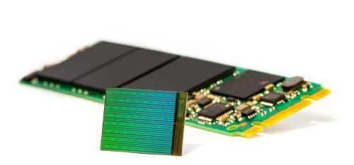
 Rambus is developing memory controller chips, expanding its business beyond just creating IP for the memory and security markets, is the latest in a stream of public disclosures and behind-the-scenes deals that have been underway for the past 18 months. And while the Rambus move is significant by itself, in the context of all the other moves over the past 18 months it blends into a landscape of equally dramatic changes.
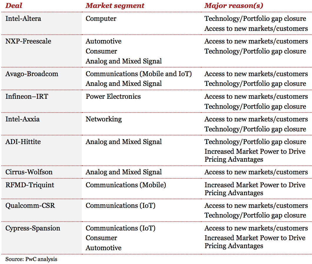
A just-released PricewaterhouseCoopers report identified several drivers for the recent string of semiconductor industry acquisitions. Among them are access to new markets or customers, closing up gaps in portfolios, resource augmentation to enable scaling, and increased market leverage.
Screen Shot 2015-08-13 at 3.11.04 PM
“As any industry experiences slower growth and increasing cost pressures, consolidation is a natural step,” said Rakesh Mehrotra, PwC’s U.S. semiconductor advisory leader. “Semiconductor companies below $500 million are experiencing consolidation for this same reason and being acquired by larger semiconductor companies. As new applications achieve success and higher growth rate returns, we will see reduced consolidation.”
Mehrotra noted that a good part of that consolidation is being driven by a need to close up product portfolio gaps for emerging applications, such as IoT/IoE and M2M. “Companies are exploring ways to offer complete integrated solutions spanning sensing, processing, and connectivity. Many of these capabilities are being integrated into either a single-chip or a single-package to offer a more competitive solution. In addition, we see consolidation is helping companies improve their position in existing markets through scale efficiency and increased share of wallet at key customers.”
In Rambus’ case, the opportunity fits a couple of those criteria, namely access to new markets and portfolio gap closure. Jerome Nadel, the company’s chief marketing officer, said it has been getting harder and harder to create a server interface for DDR4 and top customers were asking for help. The challenge for Rambus was developing a cohesive strategy for continuing to provide IP—what Nadel calls “IP as a product and IP in a product” — while making sure it didn’t step on the toes of existing memory chip customers.
The solution was a DDR4 memory interface chipset that competes directly with companies such as IDT, China’s Montage Technology, and Inphi, but none of Rambus’ memory IP customers. At the same time, considering that Rambus has been developing IP to work with this interface technology for years, it adds another potential revenue stream to Rambus’ IP portfolio. It will be designing and selling chips for the first time using a fabless model.
“There are a couple of key market trends underway here,” said Ely Tsern, vice president of Rambus’ memory products group. “One is the big data wave, with an increase in memory, bandwidth and capacity, and there has been a big uptake in servers and data centers. The second is a transition from DDR3 to DDR4, which started last year and is seeing a rapid adoption curve. The problem, though, is that DDR4 is really hard, and it’s designed to increase in speed every year. To make that work, you need buffer chips to see an increase in speed, and there are some new fundamental challenges in the technology.”
Set in the context of the semiconductor IP industry, however, this deal isn’t all that surprising. ARM, Synopsys, Cadence, Mentor Graphics and Rambus all have been buying up IP companies that are logical extensions of their businesses into adjacent markets, such as software, security, processors, subsystems, and memory verification IP. For all of these companies, this has proven to be extremely lucrative. That accounts for a string of Cadence acquisitions, elevating the company from a virtual no-show in the IP business to the No. 4 hardware IP provider, and it puts perspective on Mentor’s concerted push into automotive software.
Even on the hardware side, these kinds of expansions are not out of the usual. NXP‘s pending acquisition of Freescale and Intel‘s pending acquisition of Altera have a similar objective of growing share in their respective chip markets. In fact, Intel sold off its FPGA business to Altera in the 1990s, and now is buying back that business plus the rest of Altera. The company also purchased Docea Power late last month, ostensibly to help with power and thermal simulation/modeling when Intel and Altera chips are integrated together.
“This is the verticalization phase of the industry,” said Patrick Moorhead, president of Moor Insights and Strategy. “We see this cycle every 7 to 10 years, where the specialists realize that the sum of the parts has more value than the parts. This is more of a solutions-oriented approach, and you see this with companies like Apple, as well as with ARM and TSMC, where you can have your part based on what is a hard macro. ARM could produce chips if it wanted to. And MIPS started out with chips, then moved to IP, and now is back to chips. Really what this comes down to is control of the investment.”
Moorhead noted that with Rambus, there was a lot of pull from server OEMs. “There was a demand for a new look and vision, and ironically it was the end customers driving this. And Rambus was already getting so far into debugging and fine-tuning that they were doing a lot of the work, anyway.”
A bigger question mark for the whole ecosystem involves offshore investments, particularly from China, which could accelerate all of these moves and force deals as defensive measures. China’s technology industry is looking to fill in gaps in its current offerings, and it is much faster to buy than to build. That has has prompted a proposed $23 billion bid by Tsinghua Unigroup, a state-owned chip design company, for Micron. According to Srini Sundararajan, analyst at Summit Research Partners, that proposal is likely to evolve into an investment rather than an acquisition due to national security concerns by the U.S. government.
And behind all of this are questions from investors about where the value will be for semiconductors over the next few years. While the declines are flattening, according to the PWC report, the reduction in ASPs from a high in 1995 and a resurgence in 2005 mean companies have to fight for fewer dollars in hardware, or pick alternative approaches in adjacent markets.
There are some bright spots, though. “For certain segments such as automotive and industrial we expect to see ASPs stabilize driven by both scale effects and the growing demand for semiconductor ICs within these applications,” said PwC’s Mehrotra. “ASPs for computing and consumer segments will continue to face downward pressure, especially for devices such as sensor ICs and low-power embedded processors which are experiencing growing volume forecasts.

http://semiengineering.com/fundamental-shifts-in-chip-business/

Monday, August 17, 2015

Apple, Intel cite gains in hiring women and minorities

Apple and Intel are both making progress in their efforts to hire more women and minorities, according to figures released by the companies this week.
In the first six months of the year, more than 43 percent of Intel’s hires in the U.S. were women and minorities, up from 32 percent at the end of 2014, the company reported in its first mid-year diversity report.
At 43 percent, Intel said it was surpassing the 40 percent diversity hiring goal it set for itself for the full year.
Apple, meanwhile, boosted its hiring of women by 65 percent globally over the past year, to 11,000, the company said in its second annual report.
Apple made gains particularly in the U.S., where nearly half of its hires since January were women, black, Hispanic, or Native American, the company said.
The lack of women and minorities in Silicon Valley has become a hot-button issue in the male-dominated technology industry. A sex discrimination lawsuit brought by former Reddit CEO Ellen Pao against her former employer has also brought attention to how women are treated in Silicon Valley.
Over the past year, other companies including Google and Facebook have started to share numbers around their hiring of women and minorities.
Companies have pledged to add more diversity to their ranks and expand their recruiting efforts. By 2020, Intel wants the diversity of its workforce to mirror the availability of workers by demographic.
The numbers released by Apple and Intel, however, show that the overall representation of minorities at the companies has not dramatically changed.
Between 2014 and 2015, Apple only grew its number of female workers from 30 percent to 31 percent.
“We are proud of the progress we’ve made, and our commitment to diversity is unwavering,” said Apple CEO Tim Cook, in the company’s report. But, he said, “we know there is a lot more work to be done.”

http://www.pcworld.com/article/2971292/business/apple-intel-cite-gains-in-hiring-women-and-minorities.html

Friday, August 14, 2015

Samsung ups the SSD ante with faster, higher capacity drives

The NAND flash SSD market is becoming as speed-obsessed as the GPU makers, and that's good news for all of us. Samsung has taken the lead from Intel with a trio of new drives sporting amazing performance.
no flash
We tested the effects of browsing with and without Flash on several major browsers. Enabling Flash is,
Read Now
Samsung has introduced three TCO-optimized, high-performance drives based on its 3D Vertical NAND (V-NAND) flash memory technology, one for each SSD form factor – 2.5-inch drive, M.2 and PCI Express card.
The top of the line is Samsung's PM1725, a half-height, half-length PCIe card capable of random read speed of up to 1,000,000 IOPS, random write performance of up to 120,000 IOPS, and sequential writes of 1,800MB/s. The card comes in 3.2TB and 6.4TB capacity, the latter of which is rated to handle five complete drive writes per day for five years. In other words, you can write about 30TB to the drive every day for five years before it would fail.
ADVERTISING
 
For contrast, Intel's new 750 Series of PCIe cards are capable of 430,000 IOPS reads, 230,000 IOPS write speed, and sequential writes of 900Mbps. And that card has 400GB capacity and sells for $389. It's not even close. This Samsung card clearly is not meant for your average user.
The PM1633 is a SAS-based SSD instead of SATA which would indicate an enterprise product as well. It has random read and write speeds of up to 160,000 and 180,000 IOPS, respectively, and sequential read and write speeds of up to 1,100MB/sec and 1,000MB/sec. It will come in a 2.5-inch form factor and will be available in 480GB, 960GB, 1.92TB and 3.84TB models.
Finally there is the PM953, an update to an earlier model, the SM951, the industry's first NVMe SSD. Even though NVMe is designed for PCIe busses, the PM953 is available in M.2 and traditional 2.5-inch form factors. The M.2 version will be available in 480GB and 960GB capacities while the 2.5-inch drive version will offer 480GB, 960TB and a 1.92TB capacity model. The company did not disclose performance specs.
Samsung didn't say when these SSDs will be available or for how much but expect it to be painful for the consumer wallet. Still, it reflects the growing capacity and increasing performance of SSD, which will eventually make its way to the consumer.

http://www.itworld.com/article/2970738/hardware/samsung-ups-the-ssd-ante-with-faster-higher-capacity-drives.html

Thursday, August 13, 2015

Wednesday, August 12, 2015

One-wire EEPROM Needs No Power


http://www.eetimes.com/document.asp?doc_id=1327383

Tuesday, August 11, 2015

First 16-die stacked NAND Flash Memory with TSV Technology - See more at: http://www.newelectronics.co.uk/electronics-news/first-16-die-stacked-nand-flash-memory-with-tsv-technology/88326/#sthash.kEYwWdmf.dpuf

Toshiba has announced the development of a 16-die (max.) stacked NAND flash memory that uses Through Silicon Via (TSV) technology. The prototype will be shown at the Flash Memory Summit 2015, being held in Santa Clara, USA.
Traditional stacked NAND flash memories are connected together with wire bonding in a package, while TSV technology uses the vertical electrodes and vias to pass through the silicon dies for the connection. This enables high-speed data input and output, and reduces power consumption.
According to Toshiba the TSV technology is capable of achieving an I/O data rate of over 1Gbps which is higher than any other NAND flash memories with a low voltage supply: 1.8V to the core circuits and 1.2V to the I/O circuits and approximately a 50% power reduction of write operations, read operations, and I/O data transfers.
This new NAND flash memory provides a solution for low latency, high bandwidth and high IOPS/Watt in flash storage applications, including high-end enterprise SSD.
A part of this applied technology was developed by the New Energy and Industrial Technology Development Organization (NEDO).
- See more at: http://www.newelectronics.co.uk/electronics-news/first-16-die-stacked-nand-flash-memory-with-tsv-technology/88326/#sthash.kEYwWdmf.dpuf


Toshiba has announced the development of a 16-die (max.) stacked NAND flash memory that uses Through Silicon Via (TSV) technology. The prototype will be shown at the Flash Memory Summit 2015, being held in Santa Clara, USA.
Traditional stacked NAND flash memories are connected together with wire bonding in a package, while TSV technology uses the vertical electrodes and vias to pass through the silicon dies for the connection. This enables high-speed data input and output, and reduces power consumption.
According to Toshiba the TSV technology is capable of achieving an I/O data rate of over 1Gbps which is higher than any other NAND flash memories with a low voltage supply: 1.8V to the core circuits and 1.2V to the I/O circuits and approximately a 50% power reduction of write operations, read operations, and I/O data transfers.
This new NAND flash memory provides a solution for low latency, high bandwidth and high IOPS/Watt in flash storage applications, including high-end enterprise SSD.
A part of this applied technology was developed by the New Energy and Industrial Technology Development Organization (NEDO).


http://www.newelectronics.co.uk/electronics-news/first-16-die-stacked-nand-flash-memory-with-tsv-technology/88326/

Monday, August 10, 2015

Samsung reduces chip sales gap with Intel

Samsung Electronics has reduced the gap with Intel, the world's No. 1 chip maker, in second-quarter chip sales, according to a U.S-based market research firm.

IC Insights said Friday the sales gap between the two semiconductor giants dropped to 16 percent in the April-June period. It said Intel's semiconductor sales were 36 percent greater than Korea's largest chip maker in 2014.

"Samsung's excellent growth rate in the second quarter put the company closer to catching Intel and becoming the world's leading semiconductor supplier," it said.

Data showed Samsung's chip sales reached $10.3 billion in the second quarter, up 10 percent from a quarter ago. But those of Intel increased only 3 percent, to $11.9 billion, compared with last quarter.

The data comes a week after Korea's leading electronics company said its second-quarter operating profit was 3.4 trillion won ($2.9 billion), the second-largest figure since the company started the semiconductor business. The company also said its quarterly chip sales reached a record high of 11.29 trillion won.

Samsung's whopping growth in chip sales is due to its success in the mobile market, according to analysts.

"Intel almost failed to meet the growing demand from the mobile industry, while Samsung succeeded in catching up with the mobile market trend," said IBK Securities analyst Lee Seung-woo.

He also attributed the company's growth to its successful memory chip business.

"While Intel was focusing on the PC market, the nation's largest tech giant has successfully shifted its focus to the DRAM and NAND Flash memory chip business," he said.

Last week, Samsung said in a regulatory filing it expects to expand memory chip production more than 10 percent in the next quarter. Announcing its second-quarter performance, the company said it will increase VNAND supply to meet surging demand for mobile memory chips.


http://www.koreatimes.co.kr/www/news/tech/2015/08/133_184421.html

Thursday, August 6, 2015

Intel targets gamers with sixth-gen 'Skylake' CPU launch


Intel targets gamers with sixth-gen 'Skylake' CPU launch

82
With mobile annihilating the mainstream PC industry, Intel knows gaming is buttering its bread. The chip giant launched its sixth-generation "Skylake" desktop processors today with two enthusiast quad-core models: the Core i7-6700K and i5-6600K. The 14-nanometer chips are unlocked for maximum overclocking (all the "K" series CPUs will be), and if you're not into that, the two new chips have fairly high base frequencies: 4.0GHz for the Core i7-6700K and 3.5GHz for the i5-6600K. Compared to similar current-gen models, prices are reasonable -- suggested retail is $350 for the i7-6700K and $243 for the i5-6600K, with street prices likely lower.
Unfortunately, the i7-6700K offers just a modest performance increase (10 percent) over last-gen Haswell i7-4790K CPUs and little, if any, advantage over the current Haswell-E i7-5820K chip. However, the Skylake models are the first 14-nanometer performance CPUs that Intel has launched, because the lower-powered Broadwell 14-nanometer desktop chips aren't aimed at gamers. The smaller transistors should help overclocking, and rumor has it that the i7-6700K can be pushed to 5GHz, which may give it an edge over current tech. At any rate, with 10-nanometer "Cannonlake" CPUs now delayed, Skylake is it until next year.
Intel also revealed a new platform for the chips, the Z170 chipset. Like Haswell-E, the Skylake models use DDR4 RAM, which is much faster than DDR3 memory, but also way more expensive. (Skylake chips won't run on Haswell-E X99 motherboards, which also use DDR4 RAM.) However, the Z170 chipset has a dual-memory controller, so you can use cheaper DDR3L memory on motherboards that support it. Another plus to the platform is new Intel HD 530 graphics, which run 20 to 40 percent faster than last-gen Intel HD. It also has 16 PCI Express 3.0 lanes, giving you more USB 3.0, graphics and storage options. And Intel just happens to have a new PCI Express 3.0-based 800GB 750 series SSD drive with read speeds up to 2,200MB/s.
Many folks expected Intel to launch more of its Skylake lineup today, including mainstream and mobile CPUs, so what happened? That was just a rumor in the first place, but Intel has narrowed down the timeline. It'll reveal more information at the Intel Developers Forum on August 18th, and launch the rest of the sixth-gen Skylake lineup sometime in Q3 2015. The mainstream chips will also see a modest performance bump over current-gen tech, but are expected to sip less power, giving future MacBooks, Ultrabooks, laptops and tablets improved battery life. Down the road, it may also reveal more high-performance desktop Skylake CPUs, hopefully including an "Extreme" model
http://www.engadget.com/2015/08/05/intel-skylake-desktop-enthusiast-cpus/

Wednesday, August 5, 2015

Samsung to cut shipment of PC DRAMs, focus on mobile

Samsung Electronics Co. plans to cut its output of PC dynamic random access memory chips and tap deeper into the mobile segment ahead of the release of U.S. Apple Inc.'s new iPhone models, industry sources said Wednesday.

Samsung is set to reduce the shipment of standard DRAMs used in personal computers, eventually by 30 percent, reported the Taiwan-based Economic Daily News, a move apparently aimed at bolstering its mobile DRAM capability.

"We cannot give details on the reduction of the production (of standard DRAMs)," a Samsung Electronics official said. "However, it is right to say we are seeking to expand sales of high-end products, such as mobile and server DRAMs."

Industry watchers said Samsung's plans are apparently tied to the upcoming release of new iPhone models slated for later this year, adding that Samsung's smaller South Korean rival SK hynix Inc. and Micron Technology Inc. in the U.S. will not be able to meet Apple's demand fully.

The South Korean tech giant accounted for 44.1 percent of the global DRAM market in the first quarter, marking the highest level since the 45 percent posted in the July-September period of 2011.

Samsung also posted an operating profit of 3.4 trillion won ($2.92 billion) from its chip business in the second quarter, up 82.8 percent on-year. It marked the first time for the chip business to rake in more than 3 trillion won in quarterly profits since the third quarter of 2010. (Yonhap)

http://www.koreaherald.com/view.php?ud=20150805000245

Tuesday, August 4, 2015

Sensors powered by energy harvesting key to IoT success - See more at: http://www.electronicsweekly.com/news/internet-of-things/sensors-powered-by-energy-harvesting-key-to-iot-success-2015-08/#sthash.osIwTpws.dpuf

Energy harvesting wireless sensors have sparked a dramatic rise in interest, since they represent a reliable and easy‑to‑install technology that delivers the essential input data on which the whole internet of things (IoT) model depends. Creating a sensor node that handles the essential data capture, processing and transmission with the minimal energy that can be harvested from the environment is a challenge.
There are three key tasks in energy harvesting wireless sensors: generating (harvesting) the required energy, sensing and processing environmental parameters (temperature, humidity, position) and wirelessly transmitting the collected information. All three tasks need to be optimised together to provide viable solutions.
Energy-efficient system design
The most common forms of energy harvested by IoT sensors are kinetic, solar and thermal (see box, opposite).
All three harvesting technologies provide comparatively small amounts of energy (typically in the microampere range). Power-optimised system design is therefore essential to enable wireless sensors based on these energy sources.
Three main tasks define the power budget of a wireless sensor node – sensor measurement, wireless transmission and idle (inactive) state. System design must balance the harvested energy with the power requirements of these tasks.
This balance can be established in two directions – either the system functionality (and hence the required power) is fixed and the harvester is scaled, or the energy delivery of the harvester is fixed and the system functionality needs to be optimised. The second case is the more common one.
The functionality described in this article has been implemented in the EnOcean STM 330 energy harvesting temperature sensor which can be extended with the HSM 100 humidity sensor
To illustrate the requirements, consider the case of a solar-based room control unit. Its main tasks are to measure temperature and humidity in a room and compare them with user-defined set points (usually target temperature only, sometimes also target humidity).
The available energy budget is limited by the available size for the solar cell (say 5cm2) and the expected minimum illumination level (200Lux for six hours).
Considering the typical performance of standard indoor solar cells, this means that we need to design the sensor system to consume less than 1µA average current.
For simplicity’s sake we will subsequently calculate based on average current under the assumption that the supply voltage is fixed to 3V. To assess the functionality boundaries, we will initially allocate the available energy equally over the three main tasks giving about 300nA of average current each for sensing, wireless transmission and sleep/power loss.
An optimised temperature and humidity sensing implementation would require the equivalent of approximately 1mA current for a period of 10ms for sensor operation, data exchange between sensor and processor (via I2C or a similar bus) and initial data processing. We can then calculate the maximum number of measurements per day by comparing the available energy per day (300nA x 86.4s) with the required energy per measurement (1mA x 10ms) and find that the initial energy budget would allow for 2,592 measurements per day.
Considering that temperature and humidity change only slowly and that we need to conserve energy, we set a rate of one measurement per minute (1,440 per day).
Moving to the radio transmission, we assume an average current of 25mA for formatting and transmission of data at a rate of 125kbit/s. Based on the available power budget and the required transmission current we calculate the total possible transmission time per day which equals just over one second (or 125,000 bits/15,625 bytes) per day.
Putting this in relation to the possible number of measurements, we can identify a key constraint of energy harvesting wireless sensors – the radio protocol must be optimised for minimum size. We would need to limit the total telegram length to 10 bytes in order to transmit each measurement result in one radio telegram.
From this, it is clear that both the radio protocol and the amount of transmission need to be optimised.
Energy-optimised protocols
The payload associated with sensors is often small (a few bytes), therefore an optimised protocol must limit the transmission overhead (frame control, preamble, synchronisation, error checking) as much as possible while maintaining highly reliable communication.
Standard IP protocol (UDP over IPv6) requires more than 50 bytes of overhead; therefore native IPv6 communication is usually not possible in energy harvesting sensor applications. The power optimised ISO/IEC 14543-3-1X protocol, in contrast, requires only 12 bytes in total for the transmission of 1 byte of sensor data. Using such protocol in conjunction with an intelligent transmission strategy (transmission of significant changes only) enables even use of redundant sub-telegrams to increase transmission reliability.
Minimising sleep losses
Energy harvesting wireless sensors must be in an ultra-low power sleep state for more than 99.99% of the time. Minimising power consumption in this state is therefore absolutely essential.
Considering our design example, we have a total budget of 300nA which needs to cover processor consumption in sleep mode (with the ability for timer-based periodic wake-up) as well as losses due to leakage in the energy store.
Such a low level of power consumption is difficult to achieve, even with the latest processors, and is probably the biggest design challenge. Custom mixed-signal designs and optimised system architecture are required to address these challenges.
From wired proximity to wireless
Today, input data for the IoT is often provided by wired sensors that are locally connected to controllers and actuators.
Here, all network components are in close proximity and directly connected with each other.
This approach is well suited to local applications with limited flexibility needs where data reuse is not required.
The internet of things, in contrast, no longer requires such proximity. It allows centralised or even cloud-based data processing.
Thus, the same data can be used for several applications, driving down infrastructure cost and allowing dynamic network structures.
All of these characteristics require a second cloud, consisting of sensor and actuator nodes that can be deployed and expanded flexibly.
Nodes that use minimal energy, which they harvest from their surroundings, provide a fit-and-forget solution – they can be installed in the most inaccessible locations and relied upon to execute their task with minimal maintenance or attention.
Technologies for harvesting energy
Energy can be harvested from different sources; the most commonly used are:
  • Kinetic energy – Kinetic energy in different forms (lateral movement, rotation or vibration) has long been used to generate electrical energy using electromagnetic or piezoelectric harvesters. For most applications, the electromagnetic energy harvester is the better choice as it provides a more stable energy output at a longer life cycle without ageing effects. These harvesters generally work by changing the magnetic flux through a coil either by moving a magnet relative to the coil or by changing the flux polarity. This type of kinetic energy harvesting is the technology of choice for mechanical switches and similar applications.
  • Solar energy – Many sensor applications are powered by miniaturised solar cells. They are well suited for applications with sufficient illumination (indoor or outdoor) and often used for sensor applications such as temperature, humidity, illumination or CO2 sensors. Energy delivery can be scaled by adjusting the size of the solar cell based on the available space set by the application.
  • Thermal energy – Temperature differences can be used to generate energy based on Peltier elements. The standard application for these elements is to cool an area (such as a cooling box) when electrical energy is applied. The reverse effect – generating energy based on temperature differences – is used for thermal harvesting. The output voltage of Peltier elements depends on the temperature difference and is typically very small (20mV for °C temperature difference). Specialised electronics is therefore required to utilise this energy.
- See more at: http://www.electronicsweekly.com/news/internet-of-things/sensors-powered-by-energy-harvesting-key-to-iot-success-2015-08/#sthash.osIwTpws.dpuf

http://www.electronicsweekly.com/news/internet-of-things/sensors-powered-by-energy-harvesting-key-to-iot-success-2015-08/

Monday, August 3, 2015

Sick burn, LOSER! Nvidia recalls Shield gaming slabs over BLAZE RISK

Nvidia has today urged gamers to stop using its eight-inch Shield tablets, and send them back to base, because they are a fire risk.
Nearly 90,000 units in America and Canada have been recalled over fears they will burn players.
The US Consumer Product Safety Commission said in a recall notice that there have been four reported cases of Shield batteries overheating due to thermal runaway, including two reports of damage to people's floors after they set the tablets down.
The graphics chip giant said in an alert:
Nvidia has determined the battery in these tablets can overheat and pose a fire hazard. As part of this recall, Nvidia will be replacing the tablet.
Nvidia is asking customers to submit a claim for a replacement device. Nvidia is also asking consumers to stop using the recalled tablet, except as needed to participate in the recall and back up data. Consumers will receive a replacement tablet after registering to participate in the recall.
The affected models were sold between July 2014 and July 2015. Model numbers P1761, P1761W, and P1761WX and serial numbers 0410215901781 through 0425214604018 are considered dodgy. They were sold via GameStop stores, Amazon.com, BestBuy.com, GameStop.com, NewEgg.com, TigerDirect.com, and other websites.
Now considering the Shield only went on sale in July 2014 and we're still in July 2015, you might be under the impression that the recall affects all the Shields ever sold, but Nvidia insists this isn't so.
Nvidia added that the tablets come with two types of battery. If users go to the Settings menu, check Status, and then click the battery button they'll see it's marked either Y01 or B01. It's the Y01 battery type that's the dangerous one, and B01 users don't need to worry.
Nevertheless, the recall includes 83,000 fondleslabs sold in the US, and 5,000 sold in Canada. While Nvidia hasn't released Shield sales numbers as yet, that's got to be a fairly high percentage of the gaming tablet's sales. ®

http://www.theregister.co.uk/2015/07/31/nvidia_recall_shield_tablets_fire/