SEOUL, June 29 (Yonhap) -- South Korea's top tech giant Samsung
Electronics Co. saw the sales of dynamic random access memory (DRAM)
reach to a record level in the first quarter of this year, industry data
showed Monday, with its market share also hitting its highest since
2011.
Samsung Electronics shipped DRAM products worth US$5.28
billion in the January-March period, up 41.3 percent from a year
earlier, according to the data compiled by industry tracker IHS
Technology.
The South Korean tech firm also posted a 44.1
percent share in the global DRAM market, marking the highest level since
the 45 percent posted in the third quarter of 2011, the data also
showed.
SK hynix Inc., Samsung's smaller South Korean rival,
shipped $3.31 billion worth of DRAMs over the cited period to take up
27.6 percent of the global market. U.S.-based Micron Technology Inc.
came next by taking up 21.2 percent of the market in the first quarter
by selling $2.53 billion.
Industry watchers said Samsung
Electronics' robust performance came as the company successfully started
the mass production of 20-nano products.
Taiwan-based Nanya Technology Corp. and Winbond Electronics Corp. held 3.1 percent and 1.3 percent each, the data showed.
STMicroelectronics says it is in volume production of its first ARM
Cortex-M7 processor-based microcontrollers.
The STM32F7 range of microcontrollers takes advantage of the Cortex-M7
core’s DSP extension capabilities. It has about twice the digital-signal
processing (DSP) capability of the earlier Cortex-M4 processor. See: What’s
ARM doing in the DSP market?
This will make it useful in applications requiring high-speed or
multi-channel audio, video, wireless, motion recognition, or motor control.
In an interesting feature, the USB OTG peripheral has its own power
rail so the USB interface can continue operating while the rest of the chip is
powered at 1.8V to save power.
The dual clock domain on most peripherals allows the CPU speed to be reduced
to minimize power consumption, while keeping the clock frequency unchanged on
the communication peripherals.
The MCU’s development kit comes with STM32Cube firmware library, as well as
direct support from a wide ecosystem of software-development tool partners and
the ARM mbed online community.
Called the Discovery Kit, it is priced at $49.90, and includes WQVGA
touchscreen colour display, stereo audio, multi-sensor support, security, and
high-speed connectivity.
Together with an integrated ST-Link debugger/programmer (no need for a
separate probe), unlimited expansion capability is provided through the Arduino
Uno connectivity support and immediate access to a large choice of specialized
add-on boards.
The STM32F7 devices are in production now, in a range of package options
from a 14mm x 14mm LQFP100 to 28mm x 28mm LQFP208, plus 10mm x 10mm
0.65mm-pitch UFBGA176, 13mm x 13mm 0.8mm-pitch TFBGA216, and 5.9mm x 4.6mm
WLCSP143.
Prices start from $6.73 for the STM32F745VE in 100-pin LQFP with 512KB
on-chip Flash, for orders of 1000 units.
- See more at:
http://www.electronicsweekly.com/news/products/microprocessors/st-production-cortex-m7-super-dsp-mcus-2015-06/#sthash.0BkIvRih.dpuf
STMicroelectronics says it is in volume production of its first ARM Cortex-M7 processor-based microcontrollers.
The STM32F7 range of microcontrollers takes advantage of the
Cortex-M7 core’s DSP extension capabilities. It has about twice the
digital-signal processing (DSP) capability of the earlier Cortex-M4
processor. See: What’s ARM doing in the DSP market?
This will make it useful in applications requiring high-speed or
multi-channel audio, video, wireless, motion recognition, or motor
control.
In an interesting feature, the USB OTG peripheral has its own power
rail so the USB interface can continue operating while the rest of the
chip is powered at 1.8V to save power.
The dual clock domain on most peripherals allows the CPU speed to be
reduced to minimize power consumption, while keeping the clock frequency
unchanged on the communication peripherals.
The MCU’s development kit comes with STM32Cube firmware library, as
well as direct support from a wide ecosystem of software-development
tool partners and the ARM mbed online community.
Called the Discovery Kit, it is priced at $49.90, and includes WQVGA
touchscreen colour display, stereo audio, multi-sensor support,
security, and high-speed connectivity.
Together with an integrated ST-Link debugger/programmer (no need for a
separate probe), unlimited expansion capability is provided through the
Arduino Uno connectivity support and immediate access to a large choice
of specialized add-on boards.
The STM32F7 devices are in production now, in a range of package
options from a 14mm x 14mm LQFP100 to 28mm x 28mm LQFP208, plus 10mm x
10mm 0.65mm-pitch UFBGA176, 13mm x 13mm 0.8mm-pitch TFBGA216, and 5.9mm x
4.6mm WLCSP143.
Prices start from $6.73 for the STM32F745VE in 100-pin LQFP with 512KB on-chip Flash, for orders of 1000 units.
- See more at:
http://www.electronicsweekly.com/news/products/microprocessors/st-production-cortex-m7-super-dsp-mcus-2015-06/#sthash.0BkIvRih.dpuf
AUSTIN, Texas — Freescale’s next generation of
multicore processors will use 16nm FinFET process technology, officials
announced at the company’s annual conference, Freescale Technology
Forum (Wednesday, June 24). Two QorIQ chips, LS1048A and LS1088A, are
designed for Internet of Things networking at the edge.
The new QorIQ have eight 64-bit ARM Cortex-A53 cores running at 1.5
GHz with 2 Megabytes or L2 cache and support for DDR4 SRAM. Freescale
did not say which fab would manufacture the new process node, but
promised 16nm in mid-2016.
“The world’s networks are moving and changing faster than ever
before, driven by the convergence of extreme virtualization,
software-centric network topologies, continued expansion of the IoT, and
growing demand for increased, flexible intelligence at the network’s
edge,” Tom Deitrich, senior vice president and general manager of
Freesale’s digital networking group, said in a release.
There are tens of watts in a single networking SoC, Freescale Digital
Networking Manager Stuart Forbes told EE Times, so 16nm technology will
provide twice the performance of 28nm with a similar power envelope. As
a result, the new cores will have improved ARM capabilities and power
architecture while being able to support StarCore digital signal
processing chips (DSP).
QorIQ also has hardware acceleration in its layer one logic “to
include LTE-Advanced capabilities…[and] power benefits,” Forbes said. He
added that packet and security acceleration are also key components in
Freescale’s 16nm vision.
Freescale’s 16nm platform will be supplemented with operating systems
and BSPs from partner networks. The company does not have plans for
10nm technology, and Forbes said the following generation of process
technology will not follow mobile trends directly. It will likely be
several years before 16nm technology makes it to Freescale
microcontrollers because of difficulties implementing flash and analog
in lower-level technologies.
With the second quarter of 2015
well underway, demand for passive electronic components has waned to the
point where lead times are getting shorter—good news for anyone who is
buying these parts.
“It’s basic supply and demand economics,” says Jeff Ray, vice president of corporate product supply marketing for TTI, Inc.,
in Fort Worth, Texas. “When the business climate slows down, lead times
begin to stabilize. However, [buyers] should not confuse stabilized
lead times with available-to-sell inventory. It is still very important
for them to schedule their orders at full forecast to ensure a proper
supply chain.”
Rewind back to
2014 and the landscape was quite different. At the time, Ray says he saw
“quarter-on-quarter increases in demand” over a roughly
six-quarter-long period—an environment that’s since shifted over into
the buyer’s favor.
“In general, the
second quarter of this year can be categorized as a ‘slower’ business
climate,” says Ray. “The manufacturers’ capacity for amount of supply is
more consistent with the level of business, as opposed to what we saw
in 2014.”
Understanding the negative
impact that a sudden decrease in lead times could have on their
businesses, suppliers of passive components are looking carefully at
future demand and being “pretty cautious about bringing in lead times a
week here, and two weeks there,” says Ray, who is currently witnessing a
“flat to slight reduction” in lead times. From a capacity utilization
standpoint, passive component makers are taking a similarly cautious
approach to the market for capacitors, resistors, and other passive
products.
“Capacity levels are
within fairly normal ranges right now,” says Ray, “versus the upper-end
ranges that they were in back in 2014.”
From
a vertical business standpoint, Ray says sectors such as medical,
industrial, and transportation—and the industries that support them—all
remain strong in 2015.
“They’re not
using typical, base commodity passive products,” he points out, “but
rather those that meet industrial regulatory and/or automotive standards
(for instance, under-hood temperature specifications). “Those
components are actually still pretty robust,” says Ray, “with lead times
remaining flat to slightly extended.” Dissecting the Business Sectors
In a recent TTI passives product and market overview,
Dennis M. Zogbi wrote that passives have the highest operating margins
and represent the smallest percentage of global passive component
revenues, accounting for about 13% of global capacitor, resistor, and
inductor revenues in fiscal year 2015.
“Key
end-markets where specialty components are consumed include a myriad of
fragmented segments that can broadly be categorized under the following
designations: automotive under-the-hood electronics, specialty power
supplies, specialty lighting ballasts, defense electronics, aerospace
electronics, medical electronics, welding electronics, instrumentation
and control equipment electronics, telecommunications infrastructure
equipment, marine electronics (including undersea cable), mining
electronics, railroad electronics, nuclear power plant electronics, and
down hole pump and oil and gas equipment electronics.
According
to Zogbi, the specific criteria associated with the specialty passive
component markets are: 13% of global consumption value for all passive
components is specialty in nature; specialty component markets can
largely be found in the United States, Germany, Japan, the United
Kingdom, France, and Korea; component shipment volumes are low; and
component prices are high. In addition, he writes that component price
volatility is limited, end-product life cycles are usually five to 10
years or more, vendors have advanced technical capabilities and close
customer relationships, and “products are usually high voltage, high
frequency, or high temperature in nature, and in many instances a
combination of these criteria is inherent in the parts.” Three Trends for 2015
In 3 trends in passives for 2015,
Newark element14’s Larisa Miles writes about how passive component
makers are shifting toward products that are smaller, more reliable, and
more powerful. She points to the use of polymer and hybrid capacitors,
high-density resistors, and higher-current magnetics as the top three
trends that are currently playing out within the passives sector.
“These
three trends in particular—smaller components, higher capacities, and
polymer and hybrid capacitors—will ring especially true in the tantalum,
aluminum, and polymer verticals,” Miles writes. “As the demand for
smaller, better, faster, and stronger design solutions across a wide
range of industries surges, so will the need for passives that can keep
up. The burden will be on manufacturers and distributors to invest in
technologies that can meet those demands.”
PORTLAND, Ore. — Application processors are
the beating heart of the Internet of Things — from industrial
controllers to handheld tablets to the new emerging legions of
wearables. And with all the myriad functions performed by modern devices
there was a gaping need for heterogeneous application processors that
combined high-speed microprocessors with low-power microcontrollers,
both of which could be turned on and off at will depending on the
current function being performed. Freescale Semiconductor Inc. (Austin,
Texas) claims to have pulled off just such a heterogenous mix for
embedded designs with its long-rumored, but finally here, i.MX 7 series
of application processors.
"Freescale is not the first to come out with heterogeneous
processors — TI has done it for their OMAP [Open Multimedia Applications
Platform] for mobile applications — but Freescale is the first to do it
for embedded applications," Jim McGregor, founder and principal analyst
at TIRIAS Research (Phoenix, Arizona) told EE Times in advance of
Freescale's i.MX 7 announcement. "Freescale is taking a dual strategy,
improving their 32-bit line with this announcement, which is smart,
because most embedded applications do not need 64-bit processing.
However, they are also planning to introduce full 64-bit processors,
probably in their i.MX 8 processors, which may come out later this
year."
The i.MX 7 is heterogeneous, because if houses either a single, or
dual ARM Cortex-A7 high-performance (gigaHertz) microprocessor cores
along with a single 288-megaHertzCortex-M4 micro-controller core
(delivering 100 microWatt per megaHertz and 70 microWatt per megaHertz
respectively). All of the cores can be individually power enabled to
perform together or separately as needed. This and several other on-chip
domains all of which can be switched on or off separately enable the
i.MX 7 to burn the absolute minimum amount of power necessary to perform
the currently running job.
"The i.MX 7 series we're announcing today combines gigaHertz-class
high-performance ARM Cortex-A7 cores with a low-power Cortex-M4 core,
which together with our PF3000 power management chip meets the needs of
the most innovative Internet of Things [IoT] devices with secure, power
efficient industrial, handheld, wearable and new types of IoT
innovations inventors haven't even thought of yet," Ron Martino, Vice
President of Applications Processors and Advanced Technology Adoption
for Freescale’s MCU group told EE Times in advance of the announcement
at the Freescale Technology Forum 2015 (June 22-25, Austin Texas).
The first member of the i.MX 7 series is built with Freescale's 28
nanometer process, which has proven to be reliable, ultra low leakage,
low power architecture that Martino claimed represents a 48 percent
power savings versus its competition while in Low Power State Retention
(LPSR) mode supporting DDR self-refresh, timer or single-pin wakeup,
memory state retention and no need to reboot Linux. Full-power modes can
utilize one, two or all three cores simultaneously with the unused
cores off. Overall, Marino claimed the i.MX 7 can cut power by over
one-third for most applications, thereby extending battery life,
compared to other vendor's solutions. Power saving modes include, in
order of power — high to low — run, system idle, low power idle,
suspend, standby, sleep (LPSR), secure non-volatile storage — SNVS (that
shuts down everything except the flash containing the security keys so
that tamper protection remains on) and off.
Freescales
long-rumored, but finally here, heterogeneous ARM-based i.MX 7
application processor uses four-times less power than its predecessor,
the iMX6--as little as 250 microAmps at one volt in its Low Power State
Retention mode (LPSR).
(Source: Freescale)
The i.MX 7, which is already being evaluated for design-ins at up to
10 e-Readers, smarthome- and industrial-controller plus wearable makers,
delivers core power efficiency of 15.7 Dhrystone MIPS per milliWatt,
has hardware encryption/decryption and other security features on-chip
including elliptic curve cryptography, active tamper detection, secure
boot and hardware firewalls between on-chip modules, making it suitable
for the high-security requirements of point-of-sale devices. Its
relatively small footprint and power requirements also make it suitable
for other battery powered devices besides e-Readers, such as fitness and
health monitors, smartwatches, industrial remote monitoring and
control, and a plethora of embedded apps.
When devices are idle, but ready for instant power-up to run mode,
the i.MX 7 consumes only 250 microAmps, according to Martino and can be
awoken by an on-chip timer or a GPIO (general purpose input/output
line). The i.MX 7Dual model with dual ARM Cortex-A7 cores also has dual
Ethernet gigabit with audio-visual bridging (AVB) support. Both Single-
and Dual-A7 models include external memories interfaces for eMMC5.0,
LowPower-DDR3 and are available in 19-by-19 or 12-by-12 millimeter
packages. Both will be in full production by the fourth quarter of 2015.
Samples are available now.
Freescale's
evaluation board houses the i.MX 7Dual application processor, with dual
ARM Cortex-A7 processors plus a Cortex-M4 processors, along with the
PF3000 power management chip which supports multiple one-to-five voltage
outputs, WiFi, Bluetooth Low Energy and more.
(Source: Freescale)
The development board, which will be available when the i.MX 7 ships
this fall, contains a i.MX 7Dual, PF3000 power manager, WiFi chip,
Bluetooth low power chip, USB, GPIO, and all the usual serial
interfaces, plus a socket for the plug from an electronic paper display
and either Linux or Android preinstalled.
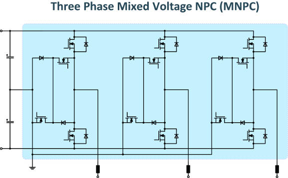
Rohm Semi and German lab Fraunhofer ISE have used SiC (silicon carbide)
transistors to squeeze a 10kW power converter into 23 x 21 x 10cm and 4,5kg.
For better efficiency, the topology chosen is mixed voltage neutral-point
clamped (MNPC,
see diagram) – also known as ‘neutral point piloted’ (NPP) and ‘T-type’,
according to the team – which has 12 transistors compared with only six needed
for a three-phase bridge consisting of three half-bridges.
All mosfets and Schottkys are silicon carbide, made by Rohm and packaged in
modules by Vincotech.
According to Rohm, compared with Si transistors, SiC allows switching
frequency to be raised 3-9x – to 100kHz in this case – shrinking the passive
components, but also increasing design challenges.
“As the high switching speed does also have an impact on the gate drive
circuits the applied driver should provide a high immunity against common mode
noise,” said the firm. “The high di/dt and du/dt during switching requires
careful design of all switching loops and nodes. Small and carefully designed
switching paths are a premise for a good SiC layout and are much more required
for SiC than for Si systems.”
BM60015FV gate drivers were used, which come in a 3.5 x 10 x 1.8mm package
with 3.75kV (VDE 0884-10 reinforced).
Using multi-mosfet modules – one per MNPC leg – reduces voltage spikes by
keeping stray inductance down compared with discrete TO-247 and TO-220
packaging – stray inductance is 5nH (+/-dc vs neutral). The modules have an
aluminium oxide base and offer 0.7K/W thermal resistance from chip to heatsink. Input
for the converter is 700-1,000Vand output is 400 at around 15Arms.
One reason for choosing MNPC topology is that not all components need to be
rated for the input voltage, allowing some lower voltage types to be used with
their inherent lower on-resistance.
In this case, for a 400V grid each of the six limbs can be made from two
650V devices (S2206 120mΩ mosfet, S6206 12A Schottky) and two 1,200V devices
(S2301 80mΩ, S6301 5A Schottky).
These are second-generation SiC mosfets, with Rohm predicting improvements
in efficiency if the design is altered for its recently introduced third
generation (double trench gate) devices.
- See more at:
http://www.electronicsweekly.com/news/design/power/sic-switching-fits-10kw-converter-five-litre-box-2015-06/#sthash.SrnDX1iV.dpuf
Intel’s purchase of Recon
Instruments, a smart eyewear company, adds to the tech company’s small
pile of investments in the fledgling wearables market. The deal (for an
undisclosed amount) was announced Thursday and follows the purchase of smartwatch maker Basis last year; the inking of a long-term deal with Luxottica for smart eyewear, including Oakley; and finally, teaming up with MICA and Opening Ceremony for smart bracelets.
Intel plans to integrate the company into its New Devices
Group, whose task is to help Intel push into a new family of smart
device platforms. Intel said it would continue selling the Recon
goggles, as well as continue designing new products.
ADVERTISING
Recon Instruments
Recon’s Snow2 smart goggles.
Some of Recon’s knowledge will be used elsewhere, too, as
Intel works hard to keep up with the evolution from the PC through
phones and tablets into the Internet of Things. “The growth of wearable
technology is creating a new playing field for innovation, and we’ve
made tremendous strides in developing products and technologies to
capture this next wave of computing,” said Josh Walden, a senior vice
president and general manager in charge of Intel’s New Technology
Group.
Dan Eisenhardt, the co-founder of Recon, said that being
brought under Intel’s wing will give them the funding to establish a
developer relations business. More importantly, however, it will give
the wearables maker access to Intel’s semiconductor design and
manufacturing expertise. At the Consumer Electronics Show in January,
Intel announced the Intel Curie embedded processor, designed to power a new generation of embedded devices.
Intel's strategy has yet to pay off with the dividends
enjoyed by Intel’s PC or server processor business. With Recon, however,
it has the option either to partner with smartglass makers—or create
its own. Why this matters: Intel’s commitment to
this brave new world of wearables is a little surprising. But if
wearables had taken off even a decade ago, they would have been powered
by the likes of Texas Instruments, Motorola, Zilog, or any number of
other embedded chip makers. Now, Qualcomm is Intel’s chief rival in this
space. By getting in on the ground floor, Intel can get its name out in
the wearables space and help drive the first few generations of
wearable designs.
PORTLAND, Ore. — Fairchild has been quietly perfecting microelectromechanical systems (MEMS) technologies since it first licensed
the Sandia (National Laboratories) Ultra Planar Multilevel MEMS
Technology (SUMMiT) for foundry services back in 2001. However, today
after over a decade of technological development, the company is
announcing its first Fairchild-branded MEMS using a "smart" technology
more sophisticated than SUMMiT, namely a six-axis inertial measurement
unit (IMU) with nine-axis sensor fusion algorithms.
Fairchild has continued filling out its "smart" MEMS technology
portfolio the easy way, by acquiring in 2010 the deep-trench high-aspect
ratio capabilities from Jyve--a serial entrepreneur Janusz Bryzek startup--and in 2014 by acquiring the Hollywood-proven motion-tracking software algorithms of Xsens.
"Fairchild knows that it is entering later a crowded space as ST,
InvenSense and more recently also Bosch have established themselves
solidly in the supply of IMUs and it can not offer a 'me-too' product,"
Jérémie Bouchaud, director and senior principal analyst, MEMS &
Sensors, at IHS told EE Times in advance of the announcement. "Therefore
Fairchild has leveraged the system and software know-how of Xsens
acquired last year to offer a lower power consumption not only at the
sensor component level but at the system level when considering the
processing power."
One "smart" aspect of Fairchild's MEMS technology is its stacked
die approach using state-of-the-art through-silicon vias (TSVs) instead
of RF interference prone wire bonding. The Jyve-inspired MEMS die, on
the bottom, and the CMOS DSP die, on the top, are stacked and packaged
in the same 3.3-by-3.3-by-1 millimeter package. The Xsens-inspired XKF3
motion processing software run on the application processor but do not
overburden it, since the data is already preprocessed by the IMU. The
chip is also self-calibrating--no more figure-eight requests of the user
by the application processor.
The new
FIS1100 MEMS chip from Fairchild cuts power by 10-fold by processing
1kHz raw data locally in its SDI (strap-down integration) AttitudeEngine
application specific integrated circuit (ASIC) mounted on top and
connected by through-silicon-vias to keep the package at just just
3-by-3-by-1 millimeter and communications to the host at just 1-to-64 Hz
through a 1536 byte first-in-first-out (FIFO).
(Source: Fairchild)
Fairchild's
MEMS is 60 microns thick using high-aspect ratio etching to produce a
low-power gyroscope that can stay one all-the-time using a single-mass
dual-cavity design for higher reliability.
(Source: Fairchild)
"Our acquisitions of Jyve and Xsens gave us the MEMS hardware and
software capabilities we needed to build a six-axis inertial measurement
unit that is both smart and low-power," Per Slycke, Senior Vice
President of Motion Tracking at Fairchild told EE Times in advance of
their announcement today. "Our IMU is smarter and up to 10-times lower
power than our competitors in the quickly growing MEMS markets for
consumer, industrial, and health applications including sports, fitness,
pedestrian navigation, autonomous robots and both virtual- and
augmented-reality."
Another "smart" aspect of Fairchild's MEMS technology is that is uses
the same die for both the accelerometer and the gyroscope, ending up
with all six-axis on the same chip. The second part of its smart MEMS
technology was to incorporate a second die it calls an SDI (for
strap-down integration, and yes, I am not kidding) which is really a
special purpose digital signal processor (DSP), dubbed an AttitudeEngine
motion processor which starts the fusion process. By reducing the
amount of raw data that needs to be sent to the application processor,
the AttitudeEngine eliminates the necessity for high-frequency
interrupts and allows the application processor to stay in sleep-mode
longer thus extending battery life. Instead of sending the raw-data
outputs from the accelerometer, gyroscope and an external magnetometer
(you buy from another vendor) the AttitudeEngine only has to send
low-bandwidth data to the host application processor, typically at just
1-to-64 Hz through its 1536 byte first-in-first-out (FIFO) buffer for
batch processing. Once the data is on the application processor,
Fairchild's Xsens XKF3 algorithms do the rest of the fusion and the
motion recognition functions.
Fairchild's
stacked ASIC attitude engine reduces overall power consumption to 0.5
microAmps compared to up to 12 microamps for competitors sending raw
data to the application processor.
(Source: Fairchild)
"Our MEMS high-aspect ratio makes its mass bigger--60 microns
thick--which results in a better signal-to-noise ratio [SNR] too,"
Slycke told us. "Our dual emphasis on high accuracy and low-power makes
the FIS1100 IMU appropriate for a wide variety of new wearable apps.
Most MEMS devices were designed for smarphones, but we're concentrating
on wearables as well as smartphones."
Fairchild claims to have the lowest power, lowest noise and best
image stabilization algorithms in the industry. Fairchild also claims
the world’s first consumer IMU with a pitch and roll accuracy of plus or
minus 3 degrees and yaw accuracy of plus or minus 5 degrees, but their
part has no announced design-ins yet so we will have to wait to see if
the proof is in the pudding.
Fairchild's
accelerometer (pictured) cast on the same MEMS die as its gyroscope,
also used its super-high 60 micron aspects ratio for low power and high
accuracy.
(Source: Fairchild)
All its algorithms are optimized for ARM processors, which it claims
dominate the wearables industry. Fairchild also provides two-versions of
a complete evaluation and development system, one of which requires an
Arduino board for its application processor, and the other of which
comes complete with an NXP application processor board onto which the
Fairchild Arduino-compatible board plugs. The Fairchild FIS1100 sensor
board also holds an AKM three-axis magnetometer to complete the
nine-axis sensor fusion.
Fairchild's
low-frequency connection to the application processor (1-to-64 Hz) is
just as accurate as a result of local processing of raw data in its
AttitudeEngine, as much higher speeds (1-kHz) which burdens the
application processor.
The semiconductor industry enjoyed a particularly strong
first quarter followed by a particularly weak second quarter, according
to Bough Lin, chairman for packaging and testing house Silicon Precision
Industries (SPIL). End market demand is unlikely to rebound until
August, said Lin.
For 2015, the semiconductor industry
should hit bottom in June-July, Lin indicated. PC sales remain sluggish
while smartphone demand in emerging markets rises at a slower pace.
Meanwhile, demand for consumer electronics devices has been weaker than
expected thus far in 2015, Lin said.
However, chip
demand will start to pick up in August and grow through October, Lin
suggested. Seasonal demand for smartphones and wearable devices will
help the industry return to its growth track in the second half of 2015,
Lin said.
In addition, Lin disclosed that SPIL's
development of system-in-package (SiP) is still lagging behind rival
Advanced Semiconductor Engineering (ASE). The target applications for
SPIL's SiP solutions will expand to include in-vehicle networking, smart
home, wearables and industrial, Lin said.
Lin also
revealed that SPIL's package-on-package (PoP) technology will be ready
for volume production between the second and third quarters of 2016.
Meanwhile, SPIL's fan-out type WLP will be available mainly for
handset-use application processors, Lin added.
SPIL's
shareholders have approved the distribution of a cash dividend per share
of NT$3 (US$0.10) for the company's 2014 operations. SPIL reported
record revenues of NT$83.07 billion for 2014, while net profits soared
99.1% on year to NT$11.73 billion. Net EPS for the year came to NT$3.76.
LED epitaxial wafer and chip maker Genesis Photonics saw
flip-chip LEDs account for 10-15% of total LED chip shipments in
first-quarter 2015 and expects the ratio to rise to 20-25% in the second
quarter and 30% in the second half of the year, according to company
chairman David Chung.
The overall utilization rate is expected to increase from 70% in the first quarter to 100% in the second quarter, Chung said.
Genesis
has become a supplier of flip-chip LEDs for LCD TV backlighting for
Samsung Electronics and also landed orders for such products from
China-based LED packaging houses in the second quarter. Genesis'
flip-chip LEDs are also being verified by LG Electronics.
Genesis expects orders for TV-backlighting applications to significantly increase in the third quarter.
Genesis
will also start producing flip-chip LEDs for automotive lighting
available in the aftermarket, including headlights and daytime running
lamps, in second-half 2015, Chung indicated.
In terms
of applications, TV backlighting accounts for 30% of Genesis' LED chip
shipments, smartphone backlighting and camera flashes 20-30%, and
lighting 40-50%.
To avoid price-cut competition with China-based makers, Genesis seeks profitability rather than revenue growth, Chung said.
In
order to reduce production cost, Genesis will begin adjusting MOCVD
combination from 80% being 2-inch tools and 20% 4-inch ones to 80%
4-inch and 20% 2-inch later in June, with the adjustment to be finished
in the third quarter, Chung indicated.
http://www.digitimes.com/news/a20150613PD201.html
Integrated Silicon Solution Inc. on Thursday said it received an
increased takeover bid from Uphill Investment Co., the latest
development in the tug of war for the chip maker.
The cash offer of $21 share, up from $20, values Integrated Silicon company at about $667
(Reuters) - Chipmaker Integrated Silicon Solutions
Inc, which rejected a bid from Cypress Semiconductor
Corp two days ago, reversed its decision on Wednesday and
said it had now agreed to Cypress's terms for the $643 million
deal to proceed.
Cypress raised its offer to buy Integrated Silicon for a
second time in May, trumping bids by a Chinese consortium led by
Uphill Investment Co.
Integrated Silicon said on Monday the deal had fallen apart
because Cypress was not willing to take "all necessary actions"
to ensure antitrust clearance in the United States and Germany.
Cypress, it said, had only agreed to take "all reasonable
actions." Both companies have a large share of the U.S. and
German SRAM memory chip market.
Integrated Silicon said on Wednesday it had now agreed to
proceed with the deal on the basis of Cypress's commitment "to
use its reasonable best efforts and take all reasonable actions"
to win antitrust approvals.
This could include fully divesting Integrated Silicon's SRAM
business if required, Integrated Silicon said.
Integrated Silicon's shares were down slightly at $20.35 in
early trading, above Cypress's offer of $20.25 per share.
Cypress shares were up 5 pct at $13.22.
SRAM (static random access memory) chips are used in a wide
range of products, including automotive electronics, appliances
and toys. They are more expensive than DRAM chips, which are
mostly used in PCs, but are faster and require less power.
Integrated Silicon, which is based in Milpitas, California,
said failure to merge with Cypress, based in San Jose, on the
terms of the current Cypress offer would reasonably be
inconsistent with its fiduciary duties under Delaware Law.
However, the company said it was still open to a
counter-offer and gave Uphill four days to come up with one.
Integrated Silicon said it delayed a special meeting of
stockholders scheduled for June 12 until at least June 19.
(Reporting by Kshitiz Goliya in Bengaluru; Editing by Saumyadeb
Chakrabarty and Ted Kerr)
TSMC has reported consolidated revenues of NT$70.16
billion (US$2.26 billion) for May 2015, representing a 15.4% increase on
year but 6.9% decrease on month.
TSMC's revenues totaled NT$367.52 billion for the first five months of 2015, rising 35.7% from a year ago.
In
other news, TSMC's board of directors has approved a capital
appropriation in the amount of approximately US$1.45 billion for the
purpose of installing advanced and specialty technology capacity,
converting certain logic capacity to specialty technologies, and for
R&D capital investments and sustaining capex in the third quarter.
The board also approved a capital injection of up to US$2 billion to
subsidiary TSMC Global for the purpose of reducing foreign exchange
hedging costs.
At a board meeting held on June 10, Morris Chang was re-elected as chairman and FC Tseng as vice chairman of TSMC.
Microsemi
has announced its Timberwolf audio processor, the ZL38AMB. It is
designed specifically for Ambarella camera SoCs and is claimed to be
engineered to be the best-in-class HD audio solution for Ambarella's
suite of video processors.
The
ZL38AMB device is designed with AcuEdge Acoustic Technology on
Microsemi's Timberwolf DSP platform, which features a set of complex,
fully integrated algorithms that allow users to extract information from
the audio environment in which they are communicating.
The audio
processor is a wideband acoustic echo canceller which also provides
noise reduction, beam forming and sound location detection for the IP
camera and wearable markets.
The ZL38AMB is said to provide voice
specific hardware accelerators, three digital microphone interfaces,
two independent 16bit D/A converters with headphone drivers and two
flexible time-division multiplexing interfaces in a single 64pin QFN or
56pin 3 x 3mm CSP. Additional features include 48kHz stereo music
playback with voice, ultra-low and standby power.
- See more at:
http://www.newelectronics.co.uk/electronics/best-in-class-audio-processor-for-iot-applications/86065/#sthash.PV2b079B.dpuf
Silicon Motion Technology has announced that its SM2256
SATA client SSD controller now supports Micron Technology's new 16nm 128
gigabit (Gb) TLC NAND flash, enabling high-performance and reliability
for cost-effective TLC-based SSDs.
Silicon Motion's
SM2256 is a four-channel SATA 6Gb/s client SSD controller built using
Micron's 128Gb 16nm TLC NAND. The new SSD controller delivers up to
540MB/s sequential read performance and 460MB/s sequential write, as
well as up to 90,000 random read IOPS and 80,000 random write IOPS.
Leveraging
Silicon Motion's proprietary NANDXtend error-correcting code (ECC)
technology, the SM2256 enhances the endurance and retention of TLC NAND,
delivering more than three times better reliability for TLC SSD as
compared to the existing BCH ECC schemes, the company said.
The
Silicon Motion SM2256 with Micron 128Gb 16nm TLC NAND is ideally suited
for client SSDs targeting ultrabooks, notebooks, tablets and HDD
replacement, Silicon Motion noted.
"Our SM2256 solution
coupled with Micron's 16nm TLC NAND delivers the most advanced,
cost-effective and reliable SSDs in the market," said Nelson Duann, VP
of product marketing for Silicon Motion. "Our customers can offer a new
class of no-compromise, cost-effective SSDs that leverage the strengths
of NAND technology advancements at affordable prices."
PORTLAND, Ore. — By moving its electronic
design automation (EDA) suite of chip-designing tools to the cloud, IBM
can now share its famous proprietary EDA tools with chip designers at
what it claims is one-half the price of licensing tools from other EDA
providers. Using its own SoftLayer cloud infrastructure to securely
store its tools, IBM is now offering its EDA toolkit through the SiCAD
Inc. (Cupertino, Calif.) portal — a silicon design platform provider of
cloud-based EDA design flows.
"We are targeting small- to medium-sized businesses, with a
factor of two in price/performance compared to other tool vendors,"
Christopher Porter, IBM high-performance computing (HPC) manager told EE
Times. "We now offer a pay-as-you-go business model instead of a
three-to-five year license agreement like the other EDA vendors."
IBM's tools are rented per day, per application, per core — a price
that will halve the cost of developing a new integrated circuit (IC),
according to IBM. However, IBM is not offering the complete design flow —
even internally they have to use third-party tools to complete a design
— but they are offering what they say is 70-to-90 percent of a typical
EDA design flow including its Library Characterization Tool (for
synthesis, sign-off timers and power analysis that it claims doubles
performance over competitors), its Logic Verification tool (that
verifies and debugs VHDL and Verilog designs 10-times faster than
competitors tools, it claims), along with its own Spice simulator.
IBM is offering its proprietary verification, library characterization and Spice tools for rent (pay-as-you-go).
(Source: IBM)
"And these are just the first three tools we are offering," Porter
told us. "Stay tuned as we will be enhancing our offerings in the
future."
According to IBM the tools it is offering through SiCAD offer
verification, simulation and regression testing, which is about 70
percent of the typical new IC design flow today and will become 90
percent of the typical design flow in the future as the industry
progresses to more advanced nodes.
"The number of design rules is going up and thus the complexity of
designs is going up, making our tools more and more important to the
semiconductor design flow," Porter told us.
IBM also claims that it has invest over 50-to-100 years of research
and development into its tools and have been using them internally for
10-to-20 years on real-world chip designs by more than 1,000 engineers
on as many as 500,000 jobs producing over 100 unique mainframe and Power
microprocessors, interconnects, application specific integrated
circuits (ASICs) and more. Other EDA toolkits are relative newbies in
comparison, IBM claims.
IBM claims its verification tool runs 10-times faster than other industry verification suites.
(Source: IBM)
It expects its tools to be used by enterprise-class organizations to
design systems-on-chip (SoCs) for mobile phones, wearables and
Internet-of-Things devices conceived by small-to-medium sized businesses
who will appreciate the cost savings of cloud-based EDA design flows.
Each user will be assigned its own server for both physical and
network isolation including firewalls and other proprietary techniques
for securing clients data. Clients need only workstations to access the
complete design flow toolkits of SiCAD, with no requirement for
licenses, data centers or IT staffs.
http://www.eetimes.com/document.asp?doc_id=1326801
Micron
Technology has expanded its flash storage portfolio with the addition
of what it calls a 'purpose built solution for cost sensitive consumer
applications seeking high performance and reliability'.
The
triple level cell (TLC) NAND device, built on Micron's 16nm process, is
said to deliver features which suit applications like USB drives and
consumer solid state drives.
"Our new TLC NAND technology meets
rising demand for reliable high capacity storage," said Kevin Kilbuck,
director of NAND planning. "We see 16nm TLC as an excellent solution for
2015 consumer applications as we drive toward 3D NAND TLC production in
2016."
- See more at:
http://www.newelectronics.co.uk/electronics-news/micron-launches-16gbyte-tlc-nand-on-16nm-process/85860/#sthash.E4kWGNY8.dpuf
Microsoft has teamed up with Toshiba in its latest push to address the
market for internet of things (IoT) products and services.
This mirrors the combination of IBM’s cloud service with ARM-based IoT
development platforms, which was announced earlier this year.
The plan is to bring together Microsoft’s Azure IoT Cloud infrastructure
with IoT applications running Toshiba’s sensors and wireless comms devices.
These include the firm’s ApP
Lite application processor, in-vehicle
driving recorders, sensors and cloud storage services.
The initial focus this year will be the transportation and logistics
market.
IoT applications make extensive use of cloud computing services for by gathering,
storing and processing data centrally.
“IoT is bringing in a dramatic technology transition that is reshaping the
nature of networks, the meaning of service, and the way we live and work,” said
Shigeyoshi Shimotsuji, corporate vice president at Toshiba.
“Bringing together the power of the Azure Services and IoT Suite with
Toshiba’s cutting edge sensor driven devices will provide a new level of data
access and business intelligence to customers,” said Nick Parker, corporate
vice president, Microsoft.
- See more at:
http://www.electronicsweekly.com/news/internet-of-things/microsoft-works-toshiba-iot-2015-06/#sthash.o8hIzcSU.dpuf
Microsoft
has teamed up with Toshiba in its latest push to address the market for
internet of things (IoT) products and services.
This mirrors the combination of IBM’s cloud service with ARM-based
IoT development platforms, which was announced earlier this year.
The plan is to bring together Microsoft’s Azure IoT Cloud
infrastructure with IoT applications running Toshiba’s sensors and
wireless comms devices.
These include the firm’s ApP Lite application processor, in-vehicle driving recorders, sensors and cloud storage services.
The initial focus this year will be the transportation and logistics market.
IoT applications make extensive use of cloud computing services for by gathering, storing and processing data centrally.
“IoT is bringing in a dramatic technology transition that
is reshaping the nature of networks, the meaning of service, and the
way we live and work,” said Shigeyoshi Shimotsuji, corporate vice
president at Toshiba.
“Bringing together the power of the Azure Services and IoT Suite with
Toshiba’s cutting edge sensor driven devices will provide a new level
of data access and business intelligence to customers,” said Nick
Parker, corporate vice president, Microsoft.
- See more
at:
http://www.electronicsweekly.com/news/internet-of-things/microsoft-works-toshiba-iot-2015-06/#sthash.o8hIzcSU.dpuf
Micron
Technology has expanded its flash storage portfolio with the addition
of what it calls a 'purpose built solution for cost sensitive consumer
applications seeking high performance and reliability'.
The
triple level cell (TLC) NAND device, built on Micron's 16nm process, is
said to deliver features which suit applications like USB drives and
consumer solid state drives.
"Our new TLC NAND technology meets
rising demand for reliable high capacity storage," said Kevin Kilbuck,
director of NAND planning. "We see 16nm TLC as an excellent solution for
2015 consumer applications as we drive toward 3D NAND TLC production in
2016."
- See more at:
http://www.newelectronics.co.uk/electronics-news/micron-launches-16gbyte-tlc-nand-on-16nm-process/85860/#sthash.E4kWGNY8.dpuf
Touchscreens are everywhere now, but they still don’t work as good as
they should. They remain frustratingly unresponsive to finger taps,
consume a lot of power, and are bulky.
So Silicon Valley chip maker Atmel is launching a new generation of touchscreen sensor chips that should lead to better touchscreens. The new MaxTouch U series touchscreen microcontroller chips will enable better performance, power consumption, and thinner screens.
The U Series chips support screens ranging from 1.2 inches (for
watches) to 10.1 inches for tablets, and everything in between. The San
Jose, Calif.-based Atmel has been making these kinds of chips for years.
With each new generation, it makes improvements in metrics like better
wake-up performance.
Touchscreen use has exploded over the past five years, and Atmel can
now package its chips in a space that measures 2.5 millimeters-by-2.6
millimeters. The new chips have features such as active stylus support,
low-power for wearables such as watches, passive stylus support (so you
can use things like pencils on a touchscreen), and a high hover distance
so that you can answer a phone call if you have a wet finger. The
touchscreen chips can sense water and reject it as a touch action. And
it works with multiple fingers, even if you are wearing gloves.
Binay Bajaj, the senior director of touch marketing, said the company’s expertise in low-power controllers
and touch engineering will enable new markets through its new touch
chips, which serve as building blocks for cool new gadgets. Atmel has
created six new MaxTouch U Series chips. The chips are available in
samples today, and production versions will be ready in the third and
fourth quarters.
Samsung
Electronics and SK hynix, the world's top two suppliers of dynamic
random access memory (DRAM) chips, plan to invest more on them because
of continued solid demand for use in mobile devices such as phones.
But
company officials and market experts say if the two raise their
production capacity, the long-term supply growth will remain constrained
due to technological complexity.
"Samsung Electronics plans to
maintain greater flexibility in the operation of our chip plants
according to the market situation. Although we are producing both memory
chips including DRAMs and NANDs, as well as logic chips, we may
increase the output of DRAMs for mobile devices to maximize short-term
profit," an official at the company said Sunday.
광고
He
stressed that as supply shift continue from DRAMs for use in
conventional PCs to those for use in mobile devices, the firm expects
chip prices to stabilize for the remainder of this year.
This
year, Samsung is busy manufacturing DRAMs for Apple's new iPhone said
Credit Suisse. Samsung mainly produces DRAMs at its plant in Giheung,
near Seoul, while it manufactures NANDs and processor chips at its
factories in Xian, China and Texas, the United States.
Samsung's
local rival SK hynix also plans to produce DRAMs using the company's
latest 21-nanometer class processing technology at its plant in Icheon,
Gyeonggi Province, near Seoul, from the latter half of this year, said
sources.
Although SK hynix focuses on profitability instead of
market share, some say it may ride the current market trend in DRAM
pricing by expanding.
Its M14 line is nearly finished with the clean room installation scheduled to be completed by the end of the second quarter.
"The
outlook for SK hynix is bright now because global DRAM supply is likely
to increase in 2016. The industry appears to be headed into another
shortage," said Credit Suisse analyst Keon Han.
Unlike Samsung,
SK hynix generates more than 80 percent of its annual revenue from
selling pure memory chips, which means that it is well-positioned to
benefit more than its rivals by expanding DRAM output.
"We remain bullish on memory stocks across the board," said Bernstein Research.
Samsung
Electronics is the leader in the DRAM mobile devices market as of the
first quarter with 52.1 percent, followed by SK hynix with 22.9 percent
and Micron Technology with 22.6 percent, according to data from market
research firm Dramexchange.


 Recon Instruments


